Showing Spotlights 65 - 72 of 158 in category All (newest first):
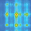 Multi-modal lasers can emit at different wavelengths simultaneously and are important for applications ranging from multiplexed signal processing to multi-color biomedical imaging. To achieve multi-wavelength capabilities, however, the single-color lasers need to be operated as an array of lasers, which dramatically increases the unit cost and precludes their integration with compact photonic devices. Researchers now have demonstrated that multi-modal lasing with control over the different colors can be achieved in a single device.
Jul 10th, 2017
 Researchers demonstrate a novel mechansim for the realization of an optical waveguide. This opens the possibility to realize a waveguide without any modulation of the refractive index. The optical delay necessary for the beam confinement is not achieved by a local modulation of the speed of light, but through an exotic effect called 'geometric phase'. Geometric phase is a temporal delay associated with changes in the propagation of light polarization, the latter corresponding roughly to the oscillation direction of the electromagnetic field.
Mar 14th, 2017
 Photodetectors with a spectral response from the ultraviolet (UV) to visible light have significant importance in modern industrial and scientific applications such as imaging, communication, environmental monitoring and day and nighttime surveillance. Compared to other materials, the photo-current conversions of two-dimensional transition metal dichalcogenides such as MoS2 nanosheets are impressive, making them great candidates for next-generation visible light photodetectors. Researchers have now developed a facile and low-cost solution processing strategy to fabricate mechanically flexible 2D organic-inorganic hybrid thin-film photodetectors on a conventional filter paper.
Mar 9th, 2017
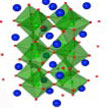 Complex oxide perovskite have been intensively researched for over half a century for their intriguing high temperature superconductivity, thermoelectric, ferroelectricity, colossal magnetoresistance. However, their large band gaps limit their interaction with visible photons. In new work, researchers propose transition metal perovskite chalcogenides (TMPCs) as a new class of versatile semiconductors for optoelectronic applications.
Feb 28th, 2017
 Compact optical components are crucial to realize miniaturized optical systems and integrated optoelectronic devices. Plasmonic metasurfaces - structured materials in 2D with rationally designed, subwavelength-scale building blocks - have drawn great interest because they can control light based on subwavelength structures. These planar devices are attractive for applications ranging from high resolution imaging to 3D holography. New work describes the design and prototyping of single-crystalline TiN plasmonic metasurfaces based on subwavelength hole arrays.
Jan 27th, 2017
 Metal nanoparticles can concentrate light near their surface through the excitation of surface plasmons, which are collective oscillations of electrons. Depending on the size and shape of the metal particles, surface plasmons can show a range of different optical responses and colors. In new work, researchers have now achieved narrow optical resonances and tailoring of the plasmonic resonance within a single system. Since each mode can be independently optimized depending on the stretching direction, their single system can cover a large wavelength bandwidth and meet specific application requirements at the same time.
Nov 29th, 2016
 Researchers have demonstrated that full-color 3D meta-holography imaging with extended viewing angles can be realized by a single layer of nanostructured metallic surface. In order to overcome the cross-talk among different colors that normally exists in current metasurface holography, the researchers introduced an off-axis illumination method to shift the holographic image in different colors and successfully reconstructed all visible colors in the imaging area. Taking advantages of the achromatic feature of the structure, the team also demonstrated full-color holography based on seven primary colors and 3D holographic imaging.
Nov 9th, 2016
 Planar optical components are crucial to realize miniaturized optical systems and integrated optoelectronic devices. In particular, metasurfaces are of great interest for applications ranging from high resolution imaging to three-dimensional holography. Achromatic metasurfaces, which can maintain the same focal distance over a range of wavelengths, have been realized by engineering each subwavelength unit to induce an identical phase change at all wavelengths. However, the design method requires intensive computation. Researchers now have developed a highly efficient, universal algorithmic method based on evolutionary principles for the design of ultra-thin achromatic lenses.
Oct 28th, 2016
 Subscribe to our Nanotechnology Spotlight feed