Showing Spotlights 57 - 64 of 158 in category All (newest first):
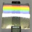 Researchers report a simple method to facilitate the mass production of flexible photonic crystals (FPCs) with full-color grating properties. The nanoimprinted FPC structure is capable of displaying full-color grating properties because of the nano-hemispherical structures on its surface. This novel approach requires relatively inexpensive equipment and much less time than previous techniques. In addition, multiple anti counterfeiting applications can be easily implemented based on the polymer's intrinsic characteristics.
Mar 19th, 2018
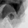 Single- or few-layer black phosphorus (BP) is one of the most promising two-dimensional semiconductors for electronic and optoelectronic device applications but its environmental instability has always posed a major hurdle for BP-based devices. In contrast, black phosphorus analogues (BPA) nanoarchitectures not only own the similar folded structure of BP, its tunable bandgap energy band and high carrier mobility, but exhibit excellent environmental stability as well. BPA nanosheets can be fabricated by a facile liquid-phase exfoliation method.
Mar 14th, 2018
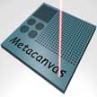 The metacanvas is a completely new generation of technology compared to all previous works. It is a tunable photonic devices based on vanadium dioxide that is lithography-free and fully reconfigurable. oth the patterns and the functionalities of the metacanvas can be arbitrarily reconfigured, which leads to many more degrees of freedom in metasurface design and functionalities. One piece of metacanvas is able to function as different optical components - hologram, phase-array, polarizer, modulator, etc. - at different times and on command, which has never been achieved in any of the previous VO2.
Feb 7th, 2018
 Plasmonic metasurfaces can be designed to achieve the singular-phase condition, yet this typically requires complex electromagnetic design and low-throughput fabrication techniques such as electron beam lithography. In a new work, researchers have developed a simple and robust planar singular-phase sensing platform for remote temperature detection, which does not require nano-patterning and exhibits singular-phase behavior due to the excitation of topologically-protected Tamm surface states.
Jan 18th, 2018
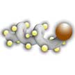 Researchers have merged two important technologies of nanomanipulation - plasmonic tweezers and magnetically driven microbots - in order to overcome their individual limitations and achieve new functionalities that did not exist before. This technique is applicable to different types of particles in various fluids. The resulting mobile nanotweezers' performance combines the best of both worlds: capturing, maneuvering, and positioning sub micrometer objects of various materials at low illumination intensities, high speeds, and with great control.
Jan 17th, 2018
 Moderate exposure to sunlight has significant health benefits, however, exposure to ultraviolet (UV) radiation also is a major risk factor for most skin cancers. That means that, while moderate exposure to sunlight is recommended, there is a fine line to walk between beneficial and harmful amounts of UV exposure. To take the guesswork out of assessing the exposure to damaging UV rays, several wearable consumer UV sensors have already hit the market. Researchers have now proposed a simple and low-cost stick-on nanoplasmonic patch made of optically active silver nanoparticles embedded in a film of nanopaper. The patch changes color once it has been exposed to a certain amount of UV light.
Nov 22nd, 2017
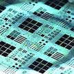 Perovskite materials have attracted great attention in the fields of optoelectronics due to their significant optoelectronic properties. So far, the applications of perovskite thin-films have been limited to solar cells because the required high-definition patterning for optoelectronic devices hadn't been achieved yet. Now, though, researchers in Korea have realized a high-resolution spin-on-patterning (SoP) process for the fabrication of optoelectronic devices arrays such as image sensors.
Sep 5th, 2017
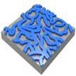 Quasi-periodic and random patterns in nature can exhibit extraordinary functions, such as iridescent color in bird wings, strong adhesion in gecko feet, and water repellency from lotus leaves. However, nature-inspired 3D nanostructures can be prohibitively expensive to make using modern nanoscale manufacturing processes. In new work, researchers a design approach integrated with scalable nanomanufacturing that can rapidly optimize and fabricate quasi-random photonic nanostructures.
Aug 1st, 2017
 Subscribe to our Nanotechnology Spotlight feed