Showing Spotlights 137 - 144 of 158 in category All (newest first):
 The success of the computer and communications industry is mainly due to the possibility of a large volume and low cost production output: silicon wafers containing myriad micro and nano structures are at the basis of Complementary Metal Oxide Semiconductor (CMOS) technology. A challenge is the realization of spatially ordered nanostructures in silicon that have many interesting applications like photonic crystals to mod the flow of light, chemical sensors, devices to alter the wetting of liquids on a surface, and as capacitors in high-frequency electronics used in mobile phones. The incorporation of such structures on existing silicon chips is greatly desired, and adapting conventional semiconductor nanofabrication to that end is widely pursued. Just a few days ago we wrote about the general aspects and challenges of silicon photonics and today we are taking a look at a specific fabrication challenge. The challenge for researchers is to to obtain photonic crystals with stop bands in the telecommunication wavelength regions, i.e.1330 nm and 1550 nm. To do that, the diameter of these pores must be smaller than 500 nm. The pore to pore distances, also referred to as pitch or interpore distance, must be well below 1 micrometer. Furthermore the depth to diameter aspect ratio of the pores must be as high as possible to obtain photonic crystals with large enough volumes. Researchers in The Netherlands now have demonstrated a method to etch arrays of nanopores in silicon with record depth-to-diameter ratios. These structures are suitable for nanophotonics and were made completely with CMOS compatible technologies, making integration of photonic structures in silicon chips feasible.
Mar 26th, 2008
 In its everlasting quest to deliver more data faster and on smaller components, the silicon industry is moving full steam ahead towards its final frontiers of size, device integration and complexity. We have covered this issue numerous times in previous Spotlights. As the physical limitations of metallic interconnects begin to threaten the semiconductor industry's future, one group of researchers and companies is betting heavily on advances in photonics that will lead to combining existing silicon infrastructure with optical communications technology, and a merger of electronics and photonics into one integrated dual-functional device. Today, silicon underpins nearly all microelectronics but the end of the road for this technology has clearly come into view. Photonics is the technology of signal processing, transmission and detection where the signal is carried by photons (light) and it is already heavily used in photonic devices such as lasers, waveguides or optical fibers. Optical technology has always suffered from its reputation for being an expensive solution, due to its use of exotic materials and expensive manufacturing processes. This prompted research into using more common materials, such as silicon, for the fabrication of photonic components, hence the name silicon photonics. Although fiber-optic communication is a well-established technology for information transmission, the challenge for silicon photonics is to manufacture low-cost information processing components. Rather than building an entirely new industrial infrastructure from scratch, the goal here is to to develop silicon photonic devices manufactured using standard CMOS techniques. A recent review paper takes a look at the state of silicon photonics and identifies the challenges that remain on the path to commercialization.
Mar 14th, 2008
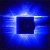 Shorter-wavelength surface-emitting laser sources are important for a variety of fields including photonics, information processing and biology. Researchers in Japan were successful in developing a current-driven blue-violet photonic crystal surface-emitting laser. They developed a fabrication method, named 'air holes retained over growth', in order to construct a two-dimensional gallium nitride/air photonic crystal structure. The resulting periodic structure has a photonic crystal band-edge effect sufficient for the successful operation of a current-injection surface-emitting laser. This represents an important step in the development of laser sources - from both a scientific and engineering point of view - that could be focused to a size much less than the wavelength and be integrated two-dimensionally at such short wavelengths.
Jan 2nd, 2008
 In October, Sony introduced the world's first OLED (organic light-emitting diode) television set. This The 11-inch OLED TV - although quite expensive at $1,700 - realizes an astonishing 3mm-thinness (at thinnest point) and unparalleled image quality. What makes OLEDs so attractive is that they do not require a backlight to function and therefore they draw far less power and, when powered from a battery, can operate longer on the same charge. OLED devices can be made thinner and lighter than comparable LED devices. Another major leap forward compared to current display technologies is that OLEDs can be printed onto almost any substrate with inkjet printer technology, making new applications like displays embedded in clothes or roll-up displays possible. Unfortunately there are also drawbacks to this technology, in particular its currently high manufacturing cost. A possible solution could lie in cost efficient mass production methods using printing or spraying techniques. These methods use semiconductor materials that are processed in the form of a dispersion, comprising soluble conjugated polymers or precursor molecules as well as colloidal, organic or inorganic nanoparticles. Inkjet-printing represents a powerful, economic tool for accurate deposition of liquids which is not only useful for graphics applications, but has also enormous potential for the direct writing of electronic devices. Researchers in Austria have now shown for the first time the highly reproducible ink-jet printing of semiconducting nanocrystals for the fabrication of optoelectronic devices.
Nov 27th, 2007
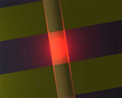
 In our Spotlight from a few weeks ago - Nanopyramids - temporary resting places for light - we wrote about things like Q-factors, qubits, stopping light and other fascinating concepts and emerging techniques that could lead to quantum computing. Some of the feedback we received could be summarized with "Huh? Q-what...?" So today we'll take another look at the Quality (Q) factor of photonic-crystal nanocavities and the context it is relevant in. These 'nanocages' for light are currently the focus of much interest of nanotechnology research in photonics because they can strongly confine photons in a tiny space. Just as semiconductor crystals control the flow of electrons (the basis for all electronics), photonic crystals are a unique material used to construct photonic devices and circuits for manipulating light, i.e. photons. A prominent example of a photonic crystal is the naturally occurring gemstone opal. Photons (behaving as waves) propagate through it - or not - depending on their wavelength. Wavelengths of light (stream of photons) that are allowed to travel throught he crystal are known as "modes". Disallowed bands of wavelengths are called photonic band gaps. What's so interesting for researchers is that, once you are able to fully control and manipulate photons, you could not only vastly improve existing applications like optical data storage, high-precision sensing and telecommunications, but develop exotic technologies like quantum computing.
Oct 1st, 2007
 Some 5,000 years ago, the megalomaniac rulers of Egypt built themselves the mothers of all tombstones - pyramids. Pyramids are the largest monuments constructed by mankind (by the way, the largest of them all, the Great Pyramid of Cholula in Mexico, has an estimated volume of 4.45 million cubic meters; which makes it almost one third larger than the Great Pyramid of Giza in Egypt; the Giza pyramid is taller, though). On the other end of the size spectrum, down to earth scientists in Germany have built some of the smallest pyramids - they are only a few hundred nanometers tall. Like their big brothers in the Arabian desert the nanopyramids' purpose is to 'entomb' something. Designed to work as a new class of microcavity optical resonator, these structures rely on internal reflection of light waves from the tilted pyramid facets to achieve strong confinement of light in all three spatial dimensions with low loss. Where the Egyptian pyramids were supposed to be a place of ascendance for the pharaoh buried inside, the German nanopyramids are 'temporary resting places' for light, giving raise to quantum optical phenomena that could provide the basis for future quantum computers.
Aug 29th, 2007
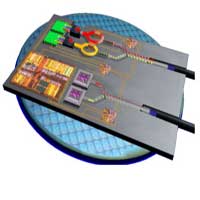
 Ever since Roman glass blowers made the Lycurgus cup, some 2,400 years ago, researchers and engineers have figured out to do all kinds of things with light, be it in optical fiber communications; the use of lasers for welding, cutting and surface modification of materials; photonic gyroscopes in aviation; or optical switches in computing. As a general field of science, photonics defines the knowledge devoted to the generation, transmission, detection, control and handling of light. One sub-domain, nanophotonics deals with the manipulation and emission of light using nanoscale material and devices. One of the sizzling hot topics within nanophotonics is plasmonics, which holds the promise of a class of subwavelength-scale optoelectronic components that could form the building blocks of a chip-based optical device technology that is scaleable to molecular dimensions. Here, we report on the latest achievements of a Spanish-French group of researchers that brings the exiting concept of an optically driven lab-on-a-chip closer.
Jul 31st, 2007
 Integrating biochemical analysis with micro- and nano-oelectromechanical systems (MEMS and NEMS) has led to the development of a new class of biomedical analytical devices called lab-on-a-chip. They combine a number of biological functions (such as enzymatic reactions, antigen-antibody conjugation, and DNA probing) with proper micro- or even nanofluidic laboratory components (such as sample dilution, pumping, mixing, metering, incubation, or separation) and detection in micron- and nanometer-sized channels and reservoirs into one single device. In order to reduce the size of these lab-on-chip devices even more, researchers increasingly are finding ways to turn micron-sized components into nanosized components. One problem they have been faced with so far is the issue of illumination. Today, many state-of-the-art lab-on-a-chip devices use external illumination sources, such as lasers or light emitting diodes (LEDs). Being able to fully integrate the excitation and detection mechanisms on lab-on-a-chip devices would allow further size reductions and increase the flexibility for using and handling them. Researchers at Cornell University have electrospun light-emitting nanofibers that, if they can be integrated with micro- and nanofluidic devices, could achieve excitation of light-induced fluorescence and detection within that same device.
May 15th, 2007
 Subscribe to our Nanotechnology Spotlight feed