Showing Spotlights 129 - 136 of 158 in category All (newest first):
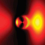 Surface-plasmon resonance is a quantum-electromagnetic phenomenon arising from the interaction of light with free electrons at the planar interface of a metal and a (nonconducting) dielectric material. This resonance arises when the energy carried by photons in the dielectric material is transferred to collective excitations (called plasmons) of free electrons in the metal at that interface. As the free electrons in the metal are coupled to the photons in the polarizable dielectric material, the quantum is called a surface plasmon-polariton (SPP). Typically, a SPP wave is launched on a metal-dielectric interface at one particular frequency. That wave has a certain polarization state. Researchers have now shown theoretically and experimentally that by modifying the dielectric material, novel surface-plasmon-polariton wave behavior can be created with the result that the same interface can independently guide more than one SPP wave.
Oct 12th, 2009
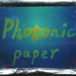 Photonic crystals are very suitable for fabricating sensor devices because the optical signals of these responsive materials are tightly coupled with various external stimuli and modulations. They could also play a significant role on the way to all-optical devices in communication and information technology - they form a basis material for the future realization of optical components and circuits, and maybe even complex optical circuits or optical computers. One application area that has seen a lot of activity recently is photonic paper and ink. One advantage of photonic papers and displays is that they are brilliant and free of glare in sunlight, which are superior to the characteristics of other emissive display technologies for outdoor usage such as advertising billboards. Another advantage is that, for recording purposes, the structural colors of photonic paper are usually more durable than traditional pigments and dyes. However, there are still a number of issues and problems that prevent the practical applications of the photonic crystal based materials. Researchers in California have now addressed some of them by reporting a new type of rewritable photonic paper on which a durable ink mark can be written or erased by introducing or removing a hygroscopic salt in the surface layer of the paper.
Aug 17th, 2009
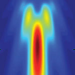 The development of electron-beam lithography, focused ion beam milling, and other nanofabrication techniques has provided researchers with great freedom to pattern metallic structures at the nanoscale. This has fueled the design and implementation of new ultracompact photonic devices based on the plasmonic behavior of metals. Plasmonics is an emerging field of nanophotonics that relies on hybrid light-charge density waves on metal-dielectric interfaces and holds the promise for control of light at dimensions much below the free-space wavelength of light. Lenses have always been an important component for controlling light in optical systems. The focusing capability of conventional, dielectric-based microlenses however deteriorates as their physical dimensions are reduced toward a single-wavelength scale. That's why scientists have begun exploring alternative approaches to refractive lensing. While nano-patterning of optically thick metallic films was theoretically proposed as an alternative to refractive lensing, scientists at Stanford University have now reported the first experimental demonstration of far-field lensing using a plasmonic slit array.
Dec 19th, 2008
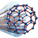
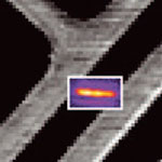 Carbon nanotubes are considered a promising material system not only for nanoelectronics but also for nanophotonics - the manipulation and emission of light using nanoscale materials and devices. By trying to understand the electrical properties of carbon nanotubes (CNTs) through their light emission, scientists are paving the way for CNTs' integration in optical applications. Embedding spatially isolated CNTs into an optical microcavity is a promising means of controlling and improving their radiative properties. The control of these CNT properties, including emission wavelength, spectral width, emission direction and radiative yield through optical confinement, opens the door for their use in integrated nanophotonic circuits. Cavity controlled nanotube emitters could potentially find use in quantum optics, quantum communication, and integrated nanophotonic circuits and may ultimately lead to low threshold on-chip nanolasers.
Sep 9th, 2008
 Photonic crystals are similar to semiconductors, only that the electrons are replaced by photons (i.e. light). By creating periodic structures out of materials with contrast in their dielectric constants, it becomes possible to guide the flow of light through the photonic crystals in a way similar to how electrons are directed through doped regions of semiconductors. The photonic band gap (that forbids propagation of a certain frequency range of light) gives rise to distinct optical phenomena and enables one to control light with amazing facility and produce effects that are impossible with conventional optics. A prominent example of a photonic crystal is the naturally occurring gemstone opal. The problem with artificial opals, which limits their applications, is that they lack in pattern variety and their fabrication requires very expensive equipment and sophisticated processes. In contrast, natural photonic crystals have various patterns that are quite promising structural matrices for creating novel optical devices. One example are peacock feathers, whose iridescent colors are derived from the 2D photonic crystals structure inside the cortex.
Aug 15th, 2008
 Optical imaging of materials is full with rich physical, chemical and biological information about the sample, because the optical energies in the visible range coincide with the atomic and molecular transition energies of many materials. Apart from the topographical information, the optical image therefore contains information about intrinsic properties of a material. However, the wave nature of light prevents the light to focus in a volume smaller than half of the wavelength, which is about 200-300 nm for visible light. Therefore, it is almost impossible to image nanomaterials, which could be a few nanometers in size, using optical imaging process. A typical lens made of, for example glass, will not be sufficient to image a nanomaterial. In work that gives rise to a new concept of a lens for optical imaging, scientists in Japan have proposed a lens made of silver nanorods, rather than a curved glass surface. This metallic nanolens is capable of manipulating light in such a way that an optical image of nanoscale objects can be obtained in the visible range.
Jun 17th, 2008
 Light-emitting nanostructures are widely used for optical, photonic, chemical, and biological devices. For example, fluorescent nanoparticles are useful for biological assays and as tumor markers, chemical sensors, and organic lasers, whereas one-dimensional luminescent nanowires are exploited for novel nanoscale photonic devices such as nano-lasers and nanowire scanning microscopy. While several methods to prepare organic, inorganic, and polymeric light-emitting nanostructures have been developed, the fabrication of luminescent nanoarchitectures with a tailored morphology and pattern is still challenging. Researchers in Korea have discovered that non-luminescent polystyrene can be converted into a luminescent organic material whose emitting color can be tuned from deep blue to white by electron irradiation. They demonstrated that luminescent nanopatterns are readily fabricated only by irradiating an electron beam to the selected regions of polystyrene. In addition, the top-down irradiation approach in conjunction with self-assembled polystyrene nanostructures allows fabrication of diverse and complex luminescent nanoarchitectures.
Jun 12th, 2008
 A key challenge in nano-optics is to bring light to and collect light from nano-scale systems. In conventional electronics, the interconnect between locally stored and radiated signals, for example radio broadcasts, is formed by antennas. For an antenna to work at the wavelength of light it needs to be greatly scaled down, to the nanoscale. Antennas play a key role in our modern wireless society. The electromagnetic waves sent and received by antennas are the messages that enable communication between electronics. Antennas with a wide variety of sizes make it possible for us receive radio broadcasts, watch television and talk to others on a mobile phone. For an effective communication, the antenna needs to direct signals towards their intended target and, vice versa, collect signals from a desired source. Now, researchers have shown that the concept of an antenna is equally well applied to direct the visible light sent out by a single molecule. For an antenna to work with visible light, it needs to be millions of times smaller than a conventional antenna. In this case, it is only 80 nanometer long. By placing the antenna near an individual molecule the light from that molecule is re-directed; the molecular message can be steered to a desired target, making efficient communication possible.
Mar 27th, 2008
 Subscribe to our Nanotechnology Spotlight feed