Showing Spotlights 121 - 128 of 158 in category All (newest first):
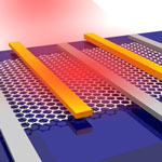
 Silicon and III-V semiconductors are the respective foundations of modern electronics and photonics. Integrating these materials is essential for achieving new optoelectronic functionality and faster computer architecture. However, lattice mismatch and high III-V growth temperatures have prevented such integration thus far. Most importantly, in order to be able to take advantage of today's massive silicon infrastructure, integration must be compatible with current complementary metal-oxide-semiconductor (CMOS) infrastructure and process flows. Researchers at UC Berkeley have overcome these obstacles by developing a way to grow III-V nanolasers on silicon, demonstrating the potency of bottom-up nano-optoelectronic integration.
Feb 22nd, 2011
 One of the many fascinating concepts in nanotechnology is the vision of molecular electronics where researchers are investigating nanostructured materials to build electronics from individual molecules. If realized, the shift in size from even the most densely packed computer chip today would be staggering. Molecular electronics aims at the fundamental understanding of charge transport through molecules and is motivated by the vision of molecular circuits to enable miniscule, powerful and energy efficient computers. A research team in Germany has now demonstrated that rigidly wired molecules can emit light under voltage bias. This result is important for fundamental science but it also adds to the molecular electronics vision an optoelectronic component, i.e. the development of optoelectronic components on the basis of single molecules.
Nov 29th, 2010
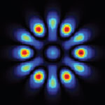
 Aberrations in optical systems, which leads to blurring of the image, and their elimination using adaptive optics have been studied in astronomical research for quite a long time. Aberrations occur when light from one point of an object after transmission through the optical system does not converge into a single point. The complicated part in correcting this error usually lies in identifying the aberrations that need to be eliminated from the system. With the emergence of nanoscale applications, aberrations in modern microscopy have become a severe limitation on the optimal performance in imaging, nanosurgery, nanofabrication and micromanipulation, just to name a few. Researchers have now demonstrated a powerful method for aberration correction with a simple implementation that typically requires minimal changes in the particular geometry.
May 25th, 2010
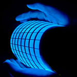 OLEDs - organic light-emitting diodes - are full of promise for a range of practical applications. OLED technology is based on the phenomenon that certain organic materials emit light when fed by an electric current and it is already used in small electronic device displays in mobile phones, MP3 players, digital cameras, and also some TV screens. With more efficient and cheaper OLED technologies it will possible to make ultra flat, very bright and power-saving OLED televisions, windows that could be used as light source at night, and large-scale organic solar cells. In contrast to regular LEDs, the emissive electroluminescent layer of an OLED consists of a thin-film of organic compounds. Exciton quenching and photon loss processes still limit OLED efficiency and brightness. Organic light-emitting transistors (OLETs) are alternative, planar light sources combining, in the same architecture, the switching mechanism of a thin-film transistor and an electroluminescent device. Thus, OLETs could open a new era in organic optoelectronics and serve as test beds to address general fundamental optoelectronic and photonic issues.
May 6th, 2010
 Silicon has dominated solid-state electronics for more than four decades but now a variety of other materials are being explored in photonic devices to expand the wavelength range of operation and to improve performance. Graphene is such a material - although most research on graphene so far has focused mainly on electronics. IBM researchers have now shown that graphene-based devices can be used in optical communications. Introducing this new material system into photonics could have a significant impact on mainstream optical applications. By using graphene, researchers make use of the internal electric field that exists at the interface of graphene and metal. Through a sophisticated combination of palladium and titanium electrodes they created a photodetector that does not rely on external current.
Apr 7th, 2010
 Spectrometers are used in materials analysis by measuring the absorption of light by a surface or chemical substance. These instruments measure properties of light over a specific portion of the electromagnetic spectrum. In conventional spectrometers, a diffraction grating splits the light source into several beams with different propagation directions according to the wavelength of the light. Thus, to achieve sufficient spatial separation for intensity measurements at a small slit, a long light path - i.e., a large instrument - is required. However, for lab-on-a-chip applications, the spectrometer must be integrated into a sub-centimeter scale device to produce a stand-alone platform. To achieve this, researchers at the Korea Advanced Institute of Science and Technology (KAIST) propose a new paradigm in which the spectrometer is based on an array of photonic crystals with different bandgaps.
Mar 8th, 2010
 A group of researchers from Singapore, led by Professor Dingyuan Tang from Nanyang Technological University and Professor Kian Ping Loh from National University of Singapore, have reported the first breakthrough in using few-layer graphene as a saturable absorber for the mode locking of lasers. Despite its prominent mechanical and electrical properties, graphene's optical response has previously been considered to be weak and featureless, so the main interests of the research community are centered on its electronics properties. But now, Tang and Loh demonstrate that graphene can be used for telecommunications applications and that its weak and universal optical response might be turned into advantages for ultrafast photonics applications.
Jan 6th, 2010
 Single molecule detection requires tools that have the detection sensitivity at the scale of single molecules. This could mean a spatial resolution requirement of only a few nanometers especially if the precise location of the molecule needs to be mapped. Researchers have already developed spectroscopic techniques capable of physical and chemical mapping on a nanometer scale. Researchers in Italy have now reported the design, fabrication and application of a photonic-plasmonic device that is fully compatible with atomic force microscopy and Raman spectroscopy - an approach that is novel in both scientific and technological aspects. The device consists of a two-dimensional dielectric photonic crystal cavity patterned on an AFM cantilever, together with a tapered silver waveguide placed at the center of the cavity.
Nov 24th, 2009
 Subscribe to our Nanotechnology Spotlight feed