Showing Spotlights 113 - 120 of 158 in category All (newest first):
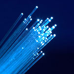 Optical fibers have revolutionized telecommunications by providing higher performance, more reliable telecommunication links with ever decreasing bandwidth cost. In parallel with these developments, fiber-optic sensor technology has been a major user of technologies associated with the optoelectronic and fiber optic communications industry. Today, with the rapid advance of communications and especially sensing applications, there is an ever increasing need for advanced performance and additional functionalities. This, however, is difficult to achieve without addressing fundamental fabrication issues related to the integration onto optical fibers of advanced functional materials at the micro- and nanoscale. Solving these technical problems will open up the possibility of developing multifunctional labs integrated onto a single optical fiber, exchanging information and combining sensorial data. This could result in auto diagnostic features as well as new photonic and electro-optic functionalities useful in many strategic sectors such as optical processing, environment, life science, safety and security.
Mar 27th, 2012
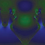
 Despite offering technological innovation in biosensing and THz metamaterials design, plasmonics faces fundamental physical limitation in the visible frequency band due to high absorptive losses of metals. The major setback to practical applications of plasmonics is high radiative and/or dissipative losses of noble-metal nanostructures in the visible frequency range. Although metal nanostructures enable unrivalled high concentration of optical energy well beyond the diffraction limit, a significant part of this energy is converted into an inherently lossy kinetic motion of free electrons in metal, and is dissipated rapidly as heat. Researchers have now demonstrated a new way to efficiently trap, enhance and manipulate light in nanoscale structures and nanopatterned thin films. This novel approach can significantly improve performance of photonic and electronic devices such as nanosensors, thin-film organic solar cells and optical nanochips.
Jan 31st, 2012
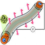 OLEDs - organic light-emitting diodes - are full of promise for a range of practical applications. OLED technology is based on the phenomenon that certain organic materials emit light when fed by an electric current and it is already used in small electronic device displays in mobile phones, MP3 players, digital cameras, and also some TV screens. OLEDs in fiber form could lead to revolutionary applications by integrating optical and optoelectronic devices into textile. Combined with nanoelectronic devices, we might one day see flexible optical sensors and display screens woven into shirts and other garments. You could literally wear your next-generation smart phone or iPad on your sleeves; including the solar panels to power them.
Jan 27th, 2012
 Fruit flies (Drosophila melanogaster) are the workhorses in countless biomedical research laboratories around the world. The bioimaging of live specimens, ideally through all the stages of the fruit fly life cycle, is a tricky and often complicated undertaking. Researchers in India have now developed a relatively simple way to introduce fluorescent nanomaterials into fruit flies: They prepared carbon nanoparticles from wood waste and added them to the flies' food supply. The fluorescent fruit flies showed no toxic effects - upon withdrawal of the nanoparticles from their food, they excreted the fluorescing material and continued to proliferate to the next generation, demonstrating a return to their normal lives.
Nov 8th, 2011
 Extracellular signaling molecules are the language that cells use to communicate with each other. These molecules transfer information not only via their chemical compositions but also through the way they are distributed in space and time throughout the cellular environment. With the development of nanosensing techniques, scientists are trying to to eavesdrop on the cellular whisper and they getting closer to deciphering extracellular signaling - an important task in understanding how cells organize themselves, for instance during organ development or immune responses. Now, researchers have reported a novel sensing technique to interrogate extracellular signaling at the subcellular level. They developed a nanoplasmonic resonator array to enhance fluorescent immunoassay signals up to more than one hundred times to enable the first time submicrometer resolution quantitative mapping of endogenous cytokine secretion from an individual cell in nanoscale close to the cell.
Aug 15th, 2011
 Exotic artificial composite materials called metamaterials can be engineered with certain electromagnetic properties that allows them to act as invisibility cloaks. These materials bend all light or other electromagnetic waves around an object hidden inside a metamaterial cloak, to emerge on the other side as if they had passed through an empty volume of space. Researchers have already been experimenting with cloaking devices for various, usually longer wavelengths such as microwave or infrared waves. Recently, even graphene has been added to the family of cloaking materials. Now, for the first time, a team of scientists at UC Berkeley have devised an invisibility cloak material that hides objects from detection using light that is visible to humans.
Aug 3rd, 2011
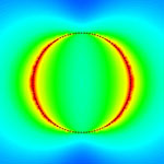
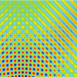
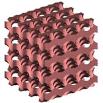 Photonic crystals are used to guide and localize light for all-optical processing of signals/information; to engineer dispersion and slow light; to harvest light (collect and redirect); and thresholdless lasing, that can be engineered by setting spectral ranges where light can be emitted. so far, there have been no demonstrations of full photonic bandgap at visible wavelengths - i.e., that at a certain visible range (between 400 nm to 780 nm) determined by the 3D photonic crystal structure, the light is rejected (reflected) at all angles of incidence. Researchers have now used a 3D nano-sculpturing process to fabricate 3D photonic crystal. The great potential of these 3D photonic crystal lies in the possibility to control light on a sub-wavelength scale.
Mar 23rd, 2011
 No matter how precise nanosensors and -probes become, bridging the huge gap between nanoscale dimensions and macroscale structures (e.g., wafer size) has been a tremendous challenge for researchers. Researchers in the U.S. have demonstrated a generalized hybrid nanofabrication concept that combines both top-down (deep-UV lithography) and bottom-up (controlled lateral epitaxial growth and atomic layer deposition) fabrication techniques. This unique methodology allows the development of reproducible nanostructured platforms that contain controlled sub-10 nm gaps between plasmonic nanostructures over an entire wafer, i.e. a 6-12 inch area. This approach opens new horizons to more widespread applications in chemical sensing and biomedical diagnostics.
Mar 2nd, 2011
 Subscribe to our Nanotechnology Spotlight feed