Showing Spotlights 81 - 88 of 158 in category All (newest first):
 Molybdenum disulfide's (MoS2) semiconducting ability, strong light-matter interaction and similarity to the carbon-based graphene makes it of interest to scientists as a viable alternative to graphene in the manufacture of electronics, particularly photoelectronics. In particular, MoS2 has excellent optical properties when deposited as a single, atom-thick layer - unlike graphene, it emits light when excited; albeit relatively poorly. In order to realize the potential of atomically thin MoS2 as a nanoscale active material in a light source, a considerable enhancement of its emission efficiency is necessary.
Mar 12th, 2015
 Polymer Dispersed Liquid Crystals (PDLCs) are micrometer-sized birefringent Liquid Crystal domains dispersed in an optically transparent continuous polymer matrix. The peculiarity of a PDLC system is that of scattering different amounts of an impinging light beam intensity, depending on the strength of an external electric field that is, eventually, applied to the system. A new generation of polymer-dispersed liquid crystals is based on a room temperature, polymerizable, nematic LC host.
Jan 13th, 2015
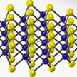 Molybdenum disulfide's (MoS2) semiconducting ability, strong light-matter interaction and similarity to graphene makes it of interest to scientists as a viable alternative in the manufacture of electronics, particularly photoelectronics. In pushing towards practical optical applications of two-dimensional (2D) MoS2, an essential gap on understanding the nonlinear optical response of 2D MoS2 and how it interacts with light, must be filled.
Oct 30th, 2014
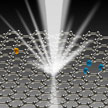 Researchers have demonstrated the experimental realization of the first all-carbon optical diode that is ready for scalable integration along with being inherently broadband in operation with no restrictions on polarization or phase-matching criteria. As they show, harnessing the optical properties of graphene-based materials offers an opportunity to create the all-photonic analogs of diodes, transistors, and photonic logic gates that will one day enable construction of the first all-photonic computer.
Sep 1st, 2014
 Aluminum has gained interest in the field of nanoplasmonics not only because it is abundant and costs a fraction of gold or silver, but also because it allows field-enhancement effects into the ultraviolet. However, it has broader resonances than silver and gold, and forms an oxide layer. Both these effects are undesirable in applications such as biosensing, in which signal strengths are reduced in the presence of resistive losses and oxide barriers. However, color printing based on the plasmon resonances of aluminum nanostructures could benefit from these properties. Researchers have now demonstrated, for the first time, the utility of aluminum nanostructures for ultrahigh definition plasmonic color printing.
Jul 15th, 2014
 The light-emitting electrochemical cell (LEC) shares several external attributes with the OLED, notably the opportunity for soft areal emission from thin-film devices, but its unique electrochemical operation eliminates the principal requirement on inert-atmosphere/vacuum processing as it can comprise solely air-stabile materials. This important intrinsic advantage has inspired recent work on an ambient-air fabrication of LEC devices using scalable means. Introducing a new, purpose-designed spray-sintering deposition technique, researchers have now shown that it is possible to spray out liquid inks onto essentially any surface for the achievement of light emission.
Jun 2nd, 2014
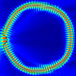
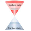 Recently, a new Dirac material - a lattice system where the excitations are described by relativistic Dirac or Weyl equations - namely a topological insulator (TI), entered researchers' sight. TIs possess a small band gap in their bulk state and a gapless metallic state at their edge/surface. A research group working on two-dimensional materials photonicshas now experimentally demonstrated for the first time that TI may be a novel microwave-absorbing material.
Apr 15th, 2014
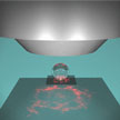 A conventional optical microscope equipped with an oil immersion objective can resolve objects no smaller than about 200 nanometers - a restriction known as the diffraction limit. The diffraction limit, which typically is half the width of the wavelength of light being used to view the specimen, represents the fundamental limit of optical imaging resolution. Breaking this limit is possible by very sophisticated techniques and costly instrumentation. Now, though, researchers in Switzerland have found that when putting a transparent dielectric particle on top of an object with nanoscale features, details of that object with a size as small as one fourth of the diffraction limit can be resolved using a conventional microscope objective.
Jan 7th, 2014
 Subscribe to our Nanotechnology Spotlight feed