Showing Spotlights 265 - 272 of 336 in category All (newest first):
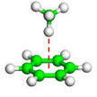
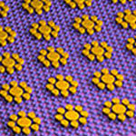
 A bacterium which causes disease reacts to the antibiotics used as treatment by becoming resistant to them, sooner or later. This natural process of adaptation, antimicrobial resistance, means that the effective lifespan of antibiotics is limited. Unnecessary use and inappropriate use of antibiotics favors the emergence and spread of resistant bacteria. New research uses a graphene-based photothermal agent to trap and kill bacteria.
Feb 19th, 2013
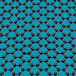
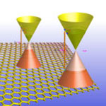
 Graphene has the potential to revolutionize many fields, especially in electronics to replace the currently used silicon materials. However, graphene does have an Achilles heel: pristine graphene is semi-metallic and lacks the necessary band gap to sever as a transistor. At present, a big challenge for graphene science is how to open a considerable band gap for graphene without significantly degrading its carrier mobility. New theoretical results suggest a rather practical solution for gap opening of graphene and silicene while preserving the desired high carrier mobility, which would allow them to serve as field effect transistors and other nanodevices.
Feb 1st, 2013
 Fuel cells are able to convert chemical energy to electrical energy with little pollutant emission and high energy conversion efficiency. Despite these advantages, the performance of fuel cells depends largely on the oxygen reduction reaction (ORR), which is substantially affected by the activity of the cathode catalyst. Since the sluggish kinetics of ORR is the major factor impeding large-scale application of fuel cells, most research focuses on developing efficient catalysts for ORR.
Dec 12th, 2012
 Within graphene research, transmission electron microscopy (TEM) has proven to be an extremely useful and versatile characterization tool. However, the electron beam can interact with the sample leading to its modification during the process. This may be an undesirable effect and measures to avoid this do exist. In other cases, however, electron beam-sample interactions can be useful for nanoengineering or nanomanufacturing. It is therefore crucially important to understand how a material responds to the electron beam and the environment inside a TEM. In new work, researchers have now demonstrated that damage-free sculpting of graphene with condensed electron beams is feasible.
Nov 12th, 2012
 Sensitive electronic devices like cell phones and computers require shielding from electromagnetic interference (EMI). Such shielding - which must be electrically conductive - has traditionally been made of metal, which poses a weight problem in the push to miniaturize and lighten electronics. Previous research has already demonstrated that ultra-lightweight carbon nanostructure-based nanocomposite materials outperform conventional metal shielding due to their light weight, resistance to corrosion, flexibility, and processing advantages. In new work, scientists in Korea have now demonstrated that single-layer graphene is an excellent choice of material for high-performance EMI shielding. They found that CVD-synthesized graphene shows more than seven times greater EMI shielding effectiveness (in terms of dB) than gold film of the same thickness.
Oct 25th, 2012
 Controlling the density of electron carriers - which are essential to the operation of electronic devices such as transistors - is achieved by doping conventional three-dimensional semiconductors. But graphene, a semi-metallic layer that is just one atom thick, has properties very different from traditional materials such as silicon. However, the doping of graphene is a key parameter in the development of graphene-based electronics. Researchers have investigated numerous strategies for doping graphene, including attaching organic or metallic molecules to its hexagonal lattice. Now, researchers have managed to dope graphene with light in a way that could lead to more efficient design and manufacture of electronics, as well as novel security and cryptography devices.
Oct 10th, 2012
 The unique energy band structure in graphene allows it to actively respond to photons with ultra-wide spectrum range - from the visible to the infrared - with record strong inter-band transition efficiency. As a consequence, graphene based ultra-fast photonics has been rising fast in various aspects of ultra-fast photonics - an ultra-fast graphene photo-detector with bandwidth exceeding 500 GHz; a broadband graphene optical modulator; a broadband graphene polarizer etc, which all benefit from the material's broadband photonics property. Researchers have now experimentally demonstrated for the first time that graphene, besides its well-known optical saturable absorption, also shows microwave and terahertz saturable absorption. The results lead to the expectation that graphene may show potential applications in microwave photonics.
Oct 2nd, 2012
 Researchers have shown that it is possible to use graphene sheets to create a superhydrophobic coating material that shows stable superhydrophobicity under both static as well as dynamic (droplet impact) conditions. They demonstrates a novel macroscopic graphene structure composed of an integrated foam-like network of graphene sheets with well-controlled microscale porosity and roughness. The novel idea here was to grow graphene over a sacrificial nickel foam template and then leech away the nickel, leaving behind a graphene foam with few-layered graphene sheets that comprise the walls of the foam. The foam is then coated with a 200nm layer of Teflon.
Sep 4th, 2012
 Subscribe to our Nanotechnology Spotlight feed