Showing Spotlights 193 - 200 of 336 in category All (newest first):
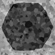
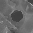 Synthesis of holey two-dimensional (2D) nanosheets with defined hole morphology and hole edge structures remains a great challenge for graphene. It is also an issue for other 2D nanomaterials, such as hexagonal boron nitride (h-BN) and molybdenum disulfide. In new work, researchers have reported a facile, controllable, and scalable method to carve geometrically defined pit/hole shapes and edges on h-BN basal plane surfaces via oxidative etching in air using silver nanoparticles as catalysts.
Oct 1st, 2015
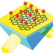 With increasing sensitivity, electrical, mechanical and optical sensors are able to detect low molecular weight chemical and biological analytes under ever more dilute conditions. At the same time, though, researchers want to keep the sensing process as simple as possible without complex functionalization and complicated preparation steps for the in situ detection. A novel graphene-gold metasurface-based biosensing architectures makes extreme phase singularities possible due to a strong field enhancement on the graphene-gold interface.
Sep 14th, 2015
 The noise level in devices with graphene and other two-dimensional (2D) materials has to be reduced in order to enable their practical applications. It will not be possible to build graphene-based communication systems or detectors until the noise spectral density is decreased to the level comparable with the conventional state-of-the-art transistors.Researchers have now demonstrated that the electronic noise in graphene devices can be strongly suppressed if a graphene channel is encased between two layers of hexagonal boron nitride.
Jul 27th, 2015
 Since the first 'Scotch tape' method - i.e. mechanical peeling - of making graphene was reported in 2004, researchers have come up with a variety of techniques for producing graphene. Since simply using the as-produced graphene flakes is not good enough for use in sophisticated applications, intricate patterning processes are essential for the development of the required graphene structures for use in nanoelectronic and optical devices. Usinf a novel method, researchers have now successfully grown graphene from neat polystyrene regions.
Jul 21st, 2015
 Researchers have demonstrated a novel, low-cost substrate processing procedure to achieve rapid, efficient synthesis of millimeter-sized single crystal graphene. One of the greatest challenges in commercializing graphene is how to produce high quality material, on an industrial scale, at low cost, and in a reproducible manner. The quality of graphene plays a crucial role as the presence of defects, impurities, domain boundaries, multiple domains, structural disorders, or wrinkles in the graphene sheet can have undesired or unexpected effects on its electronic and optical properties.
Jul 15th, 2015
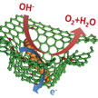 Researchers have been looking to design catalyst materials that can significantly enhance the performance of oxygen evolution reaction (OER), a key eletrode reaction that is an enabling process for many energy storage options such as direct-solar and electricity-driven water splitting and rechargeable metal-air batteries. However, OER suffers from sluggish kinetics - but a novel material inspired by the pomegranate might change that.
Jul 2nd, 2015
 Getting from 2D to 3D has been quite a challenge for the graphene community. The transfer of two-dimensional graphene onto three-dimensional surfaces has proven to be difficult due to the fractures in graphene caused by local stresses. New research is bound to change that. Scientists have demonstrated graphene integration into a variety of different microstructured geometries - pyramids, pillars, domes, inverted pyramids, as well as the integration of hybrid structure of graphene decorated with gold nanoparticles on 3D structures.
Jun 29th, 2015
 While exploring the possibility to realize graphene-like nanostructures of boron, carbon's neighbor in the periodic table, a team of chemical engineers has discovered an entirely new family of 2-D compounds. They demonstrated exfoliation of a well-known superconductor magnesium diboride, a layered material that consists Mg atoms sandwiched in between born honeycomb planes. These nanosheets can be an order of magnitude more transparent compared to their cousin graphene.
Jun 17th, 2015
 Subscribe to our Nanotechnology Spotlight feed