Showing Spotlights 129 - 136 of 336 in category All (newest first):
 Graphene bioelectronics has become a ground-breaking field that offers exciting opportunities for developing new kinds of sensors capable of establishing outstanding interfaces with soft tissue. Graphene-based transistors, as well as electrode arrays, have emerged as a special group of biosensors with their own peculiarities, advantages and drawbacks. A new review present sa comprehensive overview of the use of graphene for bioelectronics applications; specifically the focus is on interfacing graphene-based devices with electrogenic cells, such as cardiac and neuronal cells.
Sep 3rd, 2018
 Researchers have developed an all-optical lithographic technique called 'optothermoplasmonic nanolithography' (OTNL) to achieve high-throughput, versatile, and maskless patterning of different atomic layers. Taking graphene and molybdenum disulfide monolayers as examples, the team shows that both thermal oxidation and sublimation in the light-directed temperature field can lead to direct etching of the atomic layers. They further demonstrates programmable patterning of 2D materials into complex and large-scale nanostructures by steering the laser beam.
Aug 14th, 2018
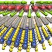
 Traditional CMOS technology cannot be directly merged with graphene applications. Photo- and electron-based lithographies, which are the main processess in today's semiconductor industry, requires use of polymers and harsh liquids that can drastically alter the initial properties of graphene. Thus graphene requires the development of novel processing technologies.
A international team of researchers now has developed a method for direct, on-the-fly reconstruction of graphene properties.
Traditional CMOS technology cannot be directly merged with graphene applications. Photo- and electron-based lithographies, which are the main processess in today's semiconductor industry, requires use of polymers and harsh liquids that can drastically alter the initial properties of graphene. Thus graphene requires the development of novel processing technologies.
A international team of researchers now has developed a method for direct, on-the-fly reconstruction of graphene properties.
Jul 30th, 2018
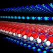 An international team of researchers has discovered a new mechanism for controlling electronic devices using molecules. The ferroelectric ordering of polar molecules attached to the edge of graphene can be toggle-switched by an electrostatic gate and can be used for memory devices and sensors. For this work, the team sandwiched graphene layers in hexagonal boron nitride crystals. The trick is to control the edge chemistry. The researchers attached different atoms to the graphene edges, before exposing them to water vapor and other polar molecules.
Jul 27th, 2018
 A new paper reviews the studies to date that have addressed the toxicity of 2D materials, particularly emphasizing the preparation methods and resulting physicochemical properties that dictate their interactions with biological systems. In addition, due to its importance in determining exposure risk, this review summarizes key results from the literature concerning the environmental fate of 2D materials. The authors hope that a thorough understanding of these issues will inform ongoing efforts to realize the design of safer 2D materials.
Jun 19th, 2018
 Although advances in optical technologies such as multi-photon microscopy and optogenetics have revolutionized researchers' ability to record and manipulate neuronal activity, integration of optical modalities with electrical recordings is challenging due to generation of light-induced artifacts. In new work, scientists report a transparent graphene microelectrode neural implant that eliminates light-induced artifacts to enable crosstalk-free integration of 2-photon microscopy, optogenetic stimulation, and cortical recordings in the same in vivo experiment.
May 24th, 2018
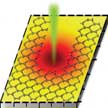
 At the nanoscale, materials become exceedingly sensitive to external perturbations. This is quite a relevant factor for wearable and flexible applications, where materials would always bear a certain degree of variable strain/stress. So far it has been very difficult to characterize strain effects in 2D materials, which is crucial to understanding strain-matter interactions. Researchers demonstrate that this limitation can be overcome by using a technique based on Kelvin Probe Microcopy.
May 9th, 2018
 Today, the common engineering solution to manufacture carbon fiber reinforced plastic composite materials is based on cross-plied carbon fibers in a polymer resin requiring high temperature cure. In contrast, researchers now have demonstrated cross-linked graphene sheets that are manufacturable from graphene platelets, which are resin-free, processable at low temperature, and contain less than 10 wt.% additives. This advance provides a universal strategy for converting inexpensive graphene platelets into high performance polymer-free graphene sheets for the development of next-generation lightweight multifunctional materials.
May 8th, 2018
 Subscribe to our Nanotechnology Spotlight feed