Showing Spotlights 225 - 232 of 318 in category All (newest first):
 'Field evaporation' is the phenomenon by which surface atoms are ionized (evaporated) under an applied, extremely high electric field of the order of several volts per nanometer. Electric fields of this magnitude can only be achieved by applying a high field to an extremely sharp needle such as the specimen tip in a Field Ion Microscope. Field evaporation was first reported over 50 years ago and has since developed into the powerful Atom Probe Field Ion Microscopy which is able to reproduce the atomic structure of a piece of material in three dimensions. Today, field evaporation is mainly used for material characterization, and the behavior of nanomaterials at extremely strong electric fields is of great scientific and technological interest. In principle, the field evaporation phenomenon can be utilized not only for materials characterization, but also for materials processing and morphology control with extremely high precision because of its unique atom-by-atom removal capability. However, detailed structural evolution of nanomaterials during field evaporation has never been directly observed and this limitation has greatly restricted the potential applications of field evaporation as a materials-processing tool. Now, researchers in Beijing have reported the first direct observation of field evaporation phenomena using a transmission electron microscopy (TEM) technique. By conducting in situ TEM field evaporation experiments on individual carbon nanotubes (CNTs), the researchers were able to reveal details about the structural evolution of the nanomaterials via direct observation. Using this technique, they have been able to perform controlled engineering of the CNTs with atomic precision, for example, grinding and shortening of CNTs, shaping of the open ends of CNTs, and opening of CNT caps.
Mar 7th, 2008
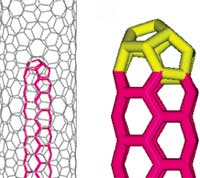 Since their discovery, the single-walled carbon nanotube (SWCNT) has evolved into one of the most intensively studied materials. A SWCNT can be regarded as a monolayer of a graphene sheet rolled up to form a seamless cylinder with axial symmetry and in general exhibiting a spiral conformation called chirality. Chirality is defined by a single vector called the chiral vector (n,m). This chiral vector is dependent on the orientation of the tube axis with respect to the hexagonal lattice. SWCNTs with different chiral vectors have dissimilar properties such as optical activity, mechanical strength and electrical conductivity. An obvious question that has been around since their discovery, but so far has not been satisfactorily answered, is how small the smallest SWCNT is. Theoretical calculations predict that the smallest diameter for a stable SWCNT is around 0.4 nm, and there are three possible structures that correspond with this value - chiral vectors (5,0), (3,3) or (4,2). Many efforts have been made to produce the smallest SWCNT and identify its atomic structure, but the techniques used were not accurate enough. Consequently, until now, the diameter and structure of the smallest possible carbon nanotube have remained in doubt. Not anymore, though. Researchers in Japan, affiliated with Sumio Iijima, the discoverer of carbon nanotubes, have successfully synthesized the smallest SWCNTs with a diameter of 0.4 nm by thermal decomposition of ferrocene molecules inside commercial-grade SWCNTs with a diameter of 1.1 nm. Apart from the scientific aspects of these findings, using the inner space of a carbon nanotube as a reaction cell appears to be an intriguing approach to fabricating new structures which would be unstable on their own.
Feb 29th, 2008
 Transparent electrical conductors pervade modern electronic devices, providing a critical component of digital cameras and video recorders, solar cells, lasers, optical communication devices, and solid-state lighting. Given the advantageous electrical properties of carbon nanotubes (CNTs), researchers already have used CNTs to impart electrical conductivity to polymeric thin films and coatings while maintaining excellent optical transparency. While this was done initially with complex lithography processes and sophisticated deposition facilities, advances in nanotube chemistry have enabled both the dissolution and dispersion of CNTs in various solvents. This has led to new alternatives for fabricating CNT patterns by simply dispensing/printing the dissolved/dispersed particles on substrates. Most methods of fabricating CNT transparent conductive film, such as vacuum filtering, laser printing, dip coating, spray coating and contact printing, require two fabrication steps to achieve the patterns. The first is to fabricate the film over all the area of the substrate. The second is to make the pattern by chemical etching or pattern transfer. In contrast, a direct printing approach has the merits of forgoing complex and expensive equipment, reducing the fabrication processes, saving the amount of material used, and removing chemical exposure in the processes. The use of off-the-shelf inkjet printers for printing patterns of carbon nanotubes on paper and plastic surfaces has been previously reported. These first inkjet demonstrations were done with multi-walled CNTs but now researchers in South Korea have managed to print pure single-walled CNTs based inkjet patterns.
Feb 26th, 2008
 Adhesive tapes are ubiquitous in our lives, whether it's on the back of a yellow sticky note, the tape that closes baby diapers, masking connectors on printed circuit boards, or surgical tape in hospitals. Most adhesive tape will stick to a wide variety of surfaces - provided that they are clean and dry. Adhesive tapes are made up of two components: a carrier which is usually paper or plastic, and an adhesive which is either water or solvent based. Many modern adhesive tapes use pressure sensitive adhesives. When you apply pressure to the tape with your finger, a strong adhesive bond is formed. Most tapes have poor ageing properties and will deteriorate quickly: with time, after several uses, or as the sticky side becomes dirty, they lose their adhesive ability. As we have reported previously, scientists are very interested in exploring the secret of the gecko's adhesive properties and to use this knowledge to create superior man-made adhesives. But it's not just the stickiness that intrigues researchers: because geckos are able to walk across a dusty or dirty surface and then scale a vertical wall without problems, their feet must also possess some kind of self-cleaning ability. Scientists have now managed to mimic the remarkable self-cleaning abilities of the gecko, as well as lotus leaves, and incorporate this ability into the design of a self-cleaning, carbon nanotube based adhesive material.
Feb 25th, 2008
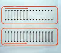
 Due to their exceptional electronic and mechanical properties, as well as their nanoscale size, carbon nanotubes (CNTs) could become the active electronic elements in addressing next generation electronic requirements for which silicon is not a solution. Already, it has been shown extensively that semiconducting CNTs can be made into electronic components such as transistors and switches. Their thermal, mechanical, chemical stability, and large current-carrying capacity make CNTs attractive for applications not only in in electrical interconnects but also field-effect transistors, cold cathode field emitters, and sensors. Some of the problems in developing CNT-based electronic devices have to do with building reliable interconnections between CNTs and external electrical and mechanical systems and in developing a reliable fabrication batch process to allow for industrial-scale mass production that supports the direct manipulation and placement/growth of CNTs at specific locations. Pointing to a possible solution, researchers now have demonstrated controllable and simultaneous wafer-scale assembly of CNT networks by dielectrophoresis.
Feb 18th, 2008
 Carbon nanotubes (CNTs) have shown promise as an important new class of multifunctional building blocks and innovative tools in a large variety of nanotechnology applications, ranging from nanocomposite materials through nanoelectronics to biomedical applications. The exploration of CNTs in biomedical applications is well underway and exploratory uses have included CNT-coated implants, drug delivery and CNTs as components of biosensors. Notwithstanding the still not satisfactorily addressed issue of toxicity, CNTs' properties such as high strength, high electrical and thermal conductivities, and high specific surface area render them particularly useful in the fabrication of nanocomposite-derived biomedical devices. In one particular area - biomaterials applied to bone - CNTs are anticipated to improve the overall mechanical properties for applications such as high-strength arthroplasty prostheses expected to remain in the body for a long time, or fixation plates and screws that will not fail or impede healing of bone. In addition, CNTs are expected to be of use as local drug delivery systems or scaffolds to promote and guide bone tissue regeneration. A new study by Japanese scientists clearly demonstrates that multi-walled CNTs (MWCNTs) have good bone-tissue compatibility, permitting bone repair and becoming closely integrated with bone tissue. Furthermore, under certain circumstances, their results indicate that MWCNTs accelerate bone formation.
Feb 15th, 2008
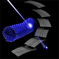 Electron microscopy is a delicate balancing act between using the highest energy electrons possible in order to obtain the best image while avoiding destruction of the sample under investigation. Trouble is, the electron beam does not just observe, it also interacts with the structure that is observed. This can be critical for fragile samples such as nanostructures: the transfer of energy from the electron beam can be sufficient that atoms are knocked right out of the material. In the worst case the sample is destroyed in front of your eyes. Scientists in Orsay, France have turned this problem to their advantage. They have developed a new approach to shaping nanomaterials atom by atom, using a scanning transmission electron microscope (STEM) as a nanometrically precise cutting tool. In this way they 'carve' their materials, such as carbon nanotubes, by removing individual atoms from specifically chosen locations. This technique has the added advantage that scientists can observe what they are doing at the same time. The new technique demonstrates a 'nanoelectron- lithography' of single walled nanotubes, a top down approach to locally control their nanostructures.
Feb 8th, 2008
 More and more carbon nanotube (CNT) applications are moving from the research lab into commercial products. For example, CNTs can be found already in tennis rackets and bicycles, displays and TV screens, and numerous resins used by aerospace, defense, health care, and electronics companies. Not surprisingly, CNT production is growing by hundreds of metric tons a year. One of the large suppliers alone, Bayer, is talking about having 3,000 metric tons of production capacity in place by 2012. As a result of the increasing supply, prices are dropping fast. While a kilogram of multi-walled CNTs (MWCNTs) sold for tens of thousands of dollars just a few years ago (and single-walled CNTs still do), the price for some types of MWCNTs has fallen to hundreds of dollars per kg. Recent market analyses forecast sales of all nanotubes to reach $1 billion to $2 billion annually within the next four to seven years. In terms of dollar value, electronics devices will be the largest end-use category, although composite materials in automotive applications may account for greater volumes. These volumes are expected to approach several thousand metric tons per year. This means that the exposure to CNTs, especially by factory workers, will increase substantially over the next few years. Since the jury is still out as to the toxicity of nanotubes it appears prudent to at least develop suitable sensor technology to detect CNTs, especially in the workplace.
Feb 4th, 2008
 Subscribe to our Nanotechnology Spotlight feed