Showing Spotlights 193 - 200 of 318 in category All (newest first):
 Pristine carbon nanotubes (CNTs) are insoluble in many liquids such as water, polymer resins, and most solvents. This means they are difficult to evenly disperse in a liquid matrix such as epoxies and other polymers, complicating efforts to utilize CNTs' outstanding physical properties in the manufacture of nanocomposite materials, as well as in other practical nanotechnology applications which require preparation of uniform mixtures of CNTs with many different organic, inorganic, and polymeric materials. To make nanotubes more easily dispersible in liquids, it is necessary to physically or chemically attach certain molecules, or functional groups, to their sidewalls without significantly changing the nanotubes' desirable properties. This process is called functionalization. Numerous nanotechnology research projects around the world are dedicated to developing various kinds of CNT-based electrochemical devices through the rational functionalization of CNTs.
Sep 17th, 2008
 Current production methods for carbon nanotubes (CNTs) result in units with different diameter, length, chirality and electronic properties, all packed together in bundles, and often blended with some amount of amorphous carbon. These mixtures are of little practical use since many advanced applications, especially for nanoelectronics, are sensitively dependent on tube structures. Consequently, the separation of metallic and semiconducting CNTs is essential for future applications and studies. The tube diameter of semiconducting nanotubes is also important because the band gap depends on it. Separation of nanotubes according to desired properties is still proving to be a challenging task, especially single-walled carbon nanotube (SWCNT) sorting, because the composition and chemical properties of SWCNTs of different types are very similar, making conventional separation techniques inefficient. The separation techniques for SWCNTs explored to date rely on preferential electron transfer on metallic SWCNTs treated with diazonium salts, dielectrophoresis, enhanced chemical affinity of semiconducting SWCNTs with octadecylamine, and wrapping of SWCNTs with single-stranded DNA.
Sep 16th, 2008
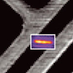 Carbon nanotubes are considered a promising material system not only for nanoelectronics but also for nanophotonics - the manipulation and emission of light using nanoscale materials and devices. By trying to understand the electrical properties of carbon nanotubes (CNTs) through their light emission, scientists are paving the way for CNTs' integration in optical applications. Embedding spatially isolated CNTs into an optical microcavity is a promising means of controlling and improving their radiative properties. The control of these CNT properties, including emission wavelength, spectral width, emission direction and radiative yield through optical confinement, opens the door for their use in integrated nanophotonic circuits. Cavity controlled nanotube emitters could potentially find use in quantum optics, quantum communication, and integrated nanophotonic circuits and may ultimately lead to low threshold on-chip nanolasers.
Sep 9th, 2008
 The demand for the raw materials of the nanotechnology revolution - nanoparticles, carbon nanotubes, fullerenes, quantum dots, etc - is rising explosively and large chemical companies keep expanding their production capacities. These industrial scale systems often depend on precious input materials and energy-hogging processes. However, there are vast amounts of 'useless' natural materials literally lying around - rocks and stones - which could find their way into nanotechnology.Researchers in Germany have made a proof of concept demonstration that using natural nanostructures found in lava rocks is suitable for nanomaterial synthesis and for use in catalysis for production of butadiene and styrene.
Sep 2nd, 2008
 Carbon nanotubes (CNTs) have been hyped as the wunderkind material of the 21st century. And while researchers have developed numerous CNT applications, ranging from nanoelectronics to nanomedicine and military armor, the actual properties of CNTs fell way short of what the theory predicted. For instance, quantum mechanics calculations predict that defect-free single-walled carbon nanotubes possess a tensile strength of well over 100 gigapascals - which translates into the ability to endure weight of over 10,000 kg on a cable with a cross-section of 1 square millimeter. In practice, CNT tensile strength of only up to 28 GPa have been measured. The problem lies not so much with the actual CNTs but rather with the mechanical tests that have been employed so far. It is very difficult to produce testable samples without damaging the tubes (which in turn adversely affects their properties), and to image the test with high enough resolution to determine the exact nature of the fracture. First experimental measurements of the mechanical properties of carbon nanotubes have now been made that directly correspond to the theoretical predictions.
Aug 14th, 2008
 Generally, a surface either loves a liquid drop (then it's called solvophilic - wetting) or hates it (called solvophobic - repulsion) when it lands, depending on several parameters of both the surface - like geometric roughness asperities or ups and downs and chemical composition - and the liquid - like surface tension or tendency of solvation. When water is the liquid the terms hydrophilic and hydrophobic are used respectively for this and for oil similar terms like oleophilic and oleophobic. Advanced material engineering techniques can structure surfaces that allow dynamic tuning of their wettability all the way from superhydrophobic behavior to almost complete wetting - but these surfaces so far only work with high-surface-tension liquids. Just recently, researchers in India have developed a superhydrophobic (where the contact angle between the droplet and the surface is approaching 180 degrees) carbon nanotube (CNT) 'bucky paper' that shows fascinating wetting behavior as a result of an applied electric field, which could be remarkably tuned by changing key solution variables like ionic strength, nature of electrolyte, and pH of the droplet.
Aug 12th, 2008
 Our title today refers to the 1960 article by Yuri Artsutanov in Pravda: 'To the Cosmos by Electric Train'. This article is the granddaddy of all 'space elevator' concepts and first to propose the idea that a cable-based transport system could become an alternative to rockets for launching people and payload into space. The single most difficult task in building the Space Elevator is achieving the required tether strength-to-weight ratio - in other words, developing a material that is both strong enough and light enough to support the up to 100,000 km long tether. Thanks to nanotechnology, this material has become available in the form of carbon nanotubes (CNTs). The challenge ahead is to weave these raw CNTs into a useful form - a space worthy climbable ribbon. Assembling carbon nanotubes into commercially usable fibers is still one of the many challenges that nanotechnology researchers are faced with when trying to exploit the amazing properties of many nanomaterials.
Aug 8th, 2008
 The success of the semiconductor industry has been due in large part to its ability to continuously increase the complexity, and therefore the processing power, of integrated circuits at a given manufacturing cost. Moore?s Law observes that the number of transistors in a computer chip doubles every two years, whilst the cost of making the chip remains the same, due to miniaturization of the components. In order to produce the next generation of computer chips it is necessary to continue to shrink the size of the components on the chip. The miniaturization upon which Moore?s Law rests has been achieved through advances in the photolithographic process used to pattern the components onto to the silicon wafer. A beam of light is projected through a shadow-casting reticule and the light pattern is then directed onto a silicon wafer coated with a photochemically sensitive material, known as a resist. The solubility of the resist is modified by exposure to the light, allowing specific areas of the resist film to be removed, whilst other areas remain as a mask, so that the silicon wafer can be selectively etched, metallized or doped. For many years it has been predicted that the end of photolithography is approaching, and that further miniaturization will require next generation lithography techniques, such as EUV lithography. However, photolithography has proved remarkably resilient, and continues to improve. Unfortunately, whilst the ability of photolithography to pattern small features continues to improve, the industry is beginning to challenge the capabilities of the photosensitive resist.
Aug 5th, 2008
 Subscribe to our Nanotechnology Spotlight feed