Showing Spotlights 145 - 152 of 318 in category All (newest first):
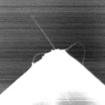 Carbon nanotubes, like the nervous cells of our brain, are excellent electrical signal conductors and can form intimate mechanical contacts with cellular membranes, thereby establishing a functional link to neuronal structures. There is a growing body of research on using nanomaterials in neural engineering. Most studies simply grow carbon nanotubes over microelectrodes to interface with neurons extracellularly. Such an extracellular interface is non-invasive, but it only allows the action potential of neurons to be recorded. In contrast, an intracellular interface allows all of the sophisticated neural activity to be probed, but it is an invasive approach that usually destroys the neuron. Now, new research by scientists in Taiwan is the first to explore the feasibility of using CNTs to probe neural activity intracellularly, opening the way for intracellular neural probes that minimize damage to the neuron.
Jul 22nd, 2009
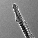 Carbon nanotubes have long been recognized as a promising material for the storage of hydrogen. Back in 2003, researchers first synthesized carbon nanoscrolls - another carbon nanomaterial similar to multi-walled carbon nanotubes - that was reported to be promising for hydrogen storage. Carbon nanoscrolls (CNS) can be obtained by rolling up a graphene sheet into a tubular structure. In contrast to multi-walled carbon nanotubes, with CNS one can vary the distance between layers, a property that might be crucial for gas storage applications. CNS are also expected to be useful in other applications, for instance in nanoelectronics, since they inherit some properties from both graphene and carbon nanotubes, e.g. high mechanical strength and carrier mobility. However, theoretical calculations also predict some unusual electronic and optical properties of CNS due to their unique topology. Previously, several methods have been developed to make CNS. However, they were hard to control, difficult to purify, and the fabricated scrolls were found to possess poor morphology. Now, researchers in Beijing have developed a simple and effective technique for fabricating high-quality CNS.
Jul 20th, 2009
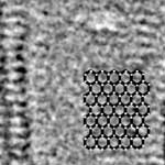
 A few days ago we ran a Nanowerk Spotlight on a nanostructuring technique that uses an extremely narrow electron beam to knock individual carbon atoms from carbon nanotubes with atomic precision, a technique that could potentially be used to change the properties of the nanotubes. In contrast to this deliberately created defect, researchers are concerned about unintentional defects created by electron beams during examination of carbon nanomaterials with transmission electron microscopes like a high-resolution transmission electron microscope (HRTEM). For a long time it has been thought that if the accelerating voltage of electrons could be reduced to 80 kV in an electron microscope, then the electrons would not possess sufficient energy to cause knock-on damage in carbon nanomaterials. Knock-on damage occurs when electrons are scattered by the nucleus of the atom they are probing. Upon scattering, energy is transferred. In some circumstances this energy can be large enough to dislodge the atom from its position. A British-German team has examined how electrons accelerated at 80 kV interact with singe-walled carbon nanotubes and shown that in some circumstances SWCNTs were unstable.
Jun 25th, 2009
 Gas sensing applications are numerous in our modern society and include process monitoring, environmental compliance, health applications, homeland security, agriculture, etc. Gas sensors often operate by detecting the subtle changes that deposited gas molecules make in the way electricity moves through a surface layer. Thus, the more surface available, the more sensitive the sensor will be. Nanoscale materials are intriguing materials for next-generation nanotechnology gas sensors since their relative surface areas are so large. A problem with existing gas nanosensors is the cross-interference of other gas analytes. For instance, carbon nanotube based gas sensors for the prominent air pollutant nitrogen dioxide have shown strong interference of ethanol and ammonia gases to the NO2 response. Another cross-interference often is caused by humidity, i.e. the water vapor in the air. New research now demonstrates how the manufacturing of a nanosensor for ammonia gas can be tuned to eliminate the interference of water vapor. The trick lies in accurately controlling the synthesis of the sensing nanomaterial.
Jun 23rd, 2009
 A broad spectrum of therapeutics or effector molecules that address several areas of medicine, from inflammation, to cancer, and regenerative medicine, are insoluble in water (they are soluble primarily in solvents generally regarded as unsuitable for injection). The water insolubility of these therapeutics limits the means by which those compounds can be administered to the body. Rapid strategies to package and disperse these drugs in biocompatible vehicles while also maintaining their potent activity can have major implications in advancing fundamental, translational, and commercial/scale-up aspects of accelerating their clinical impact. A new study now shows a way in which nanodiamonds can be applied towards enhancing water dispersion of otherwise poorly watersoluble therapeutics. It realizes a high throughout strategy to solubilize a broad range of water-insoluble drugs, which coupled with the innate biocompatibility of nanodiamonds, provides an important foundation towards a nanotechnology platform approach for advanced drug delivery.
Jun 22nd, 2009
 The manifold properties of carbon nanotubes (as well as other carbon nanomaterials such as fullerenes and graphene) are related to the various ways the carbon atoms can be arranged to form the tube lattice. Studies have shown that atomic-scale defects in these lattices can strongly influence the electronic and mechanical properties of the nanotubes. The simplest defect type is a vacancy where an atom is missing from the lattice site. Such defects can also be seen as chemically active sites for tube side wall functionalization. Due to the difficulty of observing vacancies directly, it remained unclear under what conditions vacancies in nanotubes are stable or exist at all. Researchers have now demonstrated a technique that allows them to remove carbon atoms from carbon nanotubes with atomic precision and in a controlled way with an extremely focused electron beam.
Jun 18th, 2009
 The importance of novel markers for microcopy cannot be underestimated. Such markers can provide novel information about functioning of protein in cell. Owing to their unlimited photostability diamond nanoparticles can be used for long-term monitoring of intracellular processes. Diamond nanoparticles also appear to be ideal candidates for ultra microscopy techniques like STED. Furthermore, nitrogen-vacancy color centers in diamond have non-zero spin in the ground state. This allows their use as markers for magnetic resonance imaging with very high sensitivity. To date, few methods exist to produce diamond nanoparticles containing color centers (c-diamond), but they are only laboratory-scale. The most common, large-scale nanodiamond production method, detonation, produces diamond nanoparticles which do not contain any color centers but impurities such as surface-or lattice-aggregated nitrogen and metals in significant amounts. A German-French research team has now developed a high yield method for the large-scale production of fluorescent nanodiamonds.
Jun 9th, 2009
 In a previous Spotlight we wrote about the fact that the environmental footprint created by today's nanomanufacturing technologies are conflicting with the general perception that nanotechnology is 'green' and clean. Adding to these concerns, a new study looks at the waste solids generated by the production of metallofullerenes and fullerenes and addresses the question whether feedstock-associated metals pose potential risks to aquatic receptors. The intent of this new study was to communicate that the purity of nanomaterials should be heavily characterized to ensure that the toxicological ramifications of the actual finished nanoproduct is accurately represented. Additionally, the authors suggest that carbon nanomanufacturing byproducts should be characterized so as to facilitate more informed decision-making on management of their associated waste streams.
Jun 8th, 2009
 Subscribe to our Nanotechnology Spotlight feed