Nanocrystals create 'brighter' future for TV viewers
 Researchers have discovered 'greener' nanocrystals that can be manipulated to produce high-quality pictures and lighting in electronic devices such as televisions.
Jul 8th, 2019
Read moreResearchers have discovered 'greener' nanocrystals that can be manipulated to produce high-quality pictures and lighting in electronic devices such as televisions.
Jul 8th, 2019
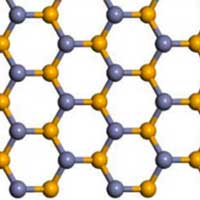
Read more A research collaboration combines theory and experimental expertise, discovering new magnetic properties of two-dimensional Fe3GeTe2 (FGT) towards spintronic applications promising faster, more efficient computing.
Jul 8th, 2019
Read more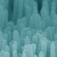 Scientists chemically treated the surface of wire-looking nanostructures made of zinc oxide to apply a uniform coating of titanium dioxide; these semiconducting nanowires could be used as high-activity catalysts for solar fuel production.
Jul 8th, 2019
Read more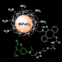 Researchers have developed a new nanotheranostic system that overcomes several problems with previous approaches.
Jul 8th, 2019
Read more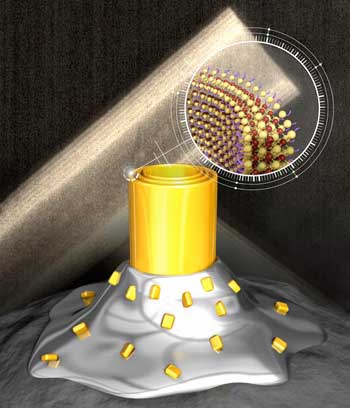 Researchers have discovered a way of making semiconducting, photoluminescent nanotubes form spontaneously in liquid solutions. The tubes, which consist of several walls that are perfectly uniform and just a few atoms thick, display optical properties that make them perfect for use as fluorophores or photocatalysts.
Jul 8th, 2019
Read more The sophisticated technology that powers face recognition in many modern smartphones someday could receive a high-tech upgrade that sounds - and looks - surprisingly low-tech.
Jul 8th, 2019
Read more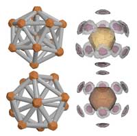 In work that upends materials design, researchers have demonstrated with computer simulations that they can design a crystal and work backward to the particle shape that will self-assemble to create it.
Jul 8th, 2019
Read more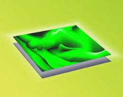 Researchers discover monolayer with exciting properties in organic semiconducting films.
Jul 8th, 2019
Read more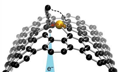 Researchers use a state-of-the-art electron microscope, the UltraSTEM, to manipulate strongly bound materials with atomic precision. Since the instruments used are fully computerized, it is possible to show in a simulation how researchers actually use them. This allows for compelling and largely realistic presentations of the most recent research in materials science.
Jul 8th, 2019
Read more The fabrication of electronic devices from exfoliated 2D materials can be tricky. Researchers have engineered a solution that consist on the after-fabrication tailoring of MoS2-FET transistors using pulsed-focused electron beam induced etching.
Jul 8th, 2019
Read more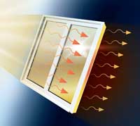 A window film with a specially designed molecule could be capable of taking the edge off the worst midday heat and instead distributing it evenly from morning to evening.
Jul 8th, 2019
Read more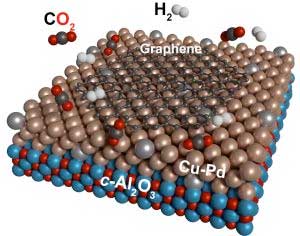 Direct conversion of greenhouse gas carbon dioxide to multi-layer graphene using copper-palladium alloys.
Jul 8th, 2019
Read more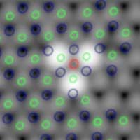 Scientists have found that the oxygen interstitials in single-layer tungsten diselenide enable it to function as single photon emitters for quantum optical applications.
Jul 8th, 2019
Read more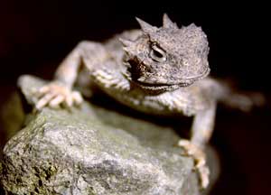 More efficient, longer-lasting machine and vehicle components, improved medical implants and novel fluid control technologies are just a few of the potential applications emerging from a project inspired by the unique ways in which the skins of some animals interact with water.
Jul 5th, 2019
Read more Self-assembling materials can form patterns that might be useful in optical devices.
Jul 5th, 2019
Read more Portable polarization-sensitive camera could be used in machine vision, autonomous vehicles, security, atmospheric chemistry and more.
Jul 5th, 2019
Read more Subscribe to our Nanotechnology News feed