Nearly two-dozen podcasts on "Materials Around Us" and "The Science of Materials" are available on Materials Radio to bring the excitement of materials to middle school students, parents and teachers.
Jan 30th, 2009
Read more
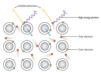 Photoelectron spectroscopy is a powerful technique for studying the composition and physical properties of a material. Despite its maturity, Yasutaka Takata from the RIKEN SPring-8 Center, Harima, and colleagues have discovered that there are still new things to learn about the physical phenomena on which it is based.
Jan 30th, 2009
Read more
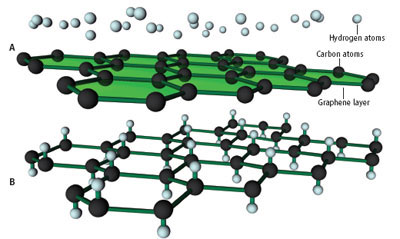 An international research team have successfully converted graphene - sheets of carbon just a single layer of atoms thick - into its hydrogenated equivalent, graphane.
Jan 30th, 2009
Read more
Senator Kim Carr, Minister for Innovation, Industry, Science and Research today released the annual report for the Australian National Nanotechnology Strategy.
Jan 30th, 2009
Read more
The federal government of Canada officially announced the 2009 budget plan and allocated a $50 million grant to the Institute for Quantum Computing (IQC) for scientific research and groundbreaking experiments.
Jan 29th, 2009
Read more
 Putting graphene sheets onto water surface reminded researchers of Monet's Water Lilies paintings.
Jan 29th, 2009
Read more
The new structure can be viewed as a NaCl-type structure, with anionic and cationic positions occupied by two different clusters of boron atoms (B12 and B2).
Jan 29th, 2009
Read more
 Individuals and startup companies now have another avenue to move their Purdue innovations to the marketplace through a new fund established by the Purdue Research Foundation and Purdue University.
Jan 29th, 2009
Read more
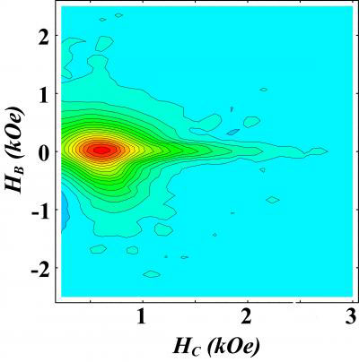
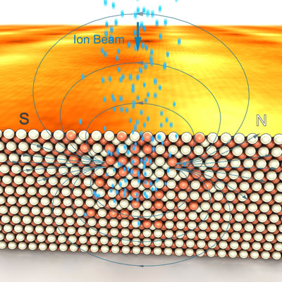 Using a highly focused ion beam, i.e. fast charged atoms, researchers have irradiated an iron-aluminum alloy in such a way that only the treated zones became ferromagnetic.
Jan 29th, 2009
Read more
Scientists at the U.S. Department of Energy's Lawrence Berkeley National Laboratory have now developed a powerful new kind of sputter process that can deposit high-quality metal films in complex, three-dimensional nanoscale patterns at a rate that by one important measure is orders of magnitude greater than typical systems
Jan 29th, 2009
Read more
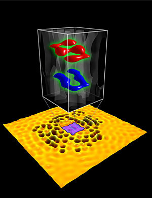
 Researchers have developed a technique to capture the magnetic "fingerprints" of certain nanostructures - even when they are buried within the boards and junctions of an electronic device.
Jan 29th, 2009
Read more
The logic and memory functions of future electronic devices could shrink dramatically - to one or two nanometers instead of the many tens of nanometers that characterize today?s most advanced elements - if a way can be found to control domain walls, the ultrathin transition zones that separate regions of a material having different magnetic, electric, or other properties.
Jan 28th, 2009
Read more
 Stanford researchers have reclaimed bragging rights for creating the world's smallest writing, a distinction the university first gained in 1985 and lost in 1990.
Jan 28th, 2009
Read more
 Scientists have found the first case of an ionic crystal consisting of just one chemical element - boron.
Jan 28th, 2009
Read more
Accumulated tribocharging in peeling tape by EM emission from nanoparticles is proposed because of the non-uniform nanosecond x-ray bursts observed in peeling Scotch tape.
Jan 28th, 2009
Read more
In the future, the interface between brain and artificial system might be based on nerve cells grown for that purpose.
Jan 28th, 2009
Read more
 Subscribe to our Nanotechnology News feed