If you are in the business of developing high-speed electronic components, it pays not to lose sight of the electrons. To keep track of them you will need to use dedicated optical elements, such as those now on offer from UltraFast Innovations GmbH.
Sep 16th, 2009
Read more
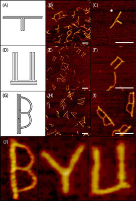 College football fans cheer when marching bands spell out the home team?s name in gigantic letters on the field at halftime. Now scientists in Utah are reporting the ultimate in one-upmanship: Development of a new technology for writing the school name in letters so small that 500 would fit across the diameter of a human hair.
Sep 16th, 2009
Read more
Physikalisch-Technische Bundesanstalt (PTB) in Berlin, Germany, has for the first time made graphene visible on gallium arsenide - A successful combination of two unique electronic materials.
Sep 16th, 2009
Read more
Tiny particles of albumin, a protein found in the blood, can be used to carry radioactive isotopes to the site of a cancerous tumour in the body and so avoid many of the side-effects of conventional radiotherapy.
Sep 16th, 2009
Read more
Organized by the Cambridge CNT Society, the 2009 forum on November 13, 2009 in Cambridge, UK, will provide a platform for reviewing and discussing novel developments in the field of carbon nanostructures and related materials as well as their applications.
Sep 16th, 2009
Read more
Der Branchendialog 'NanoEngineering' soll am 8. Dezember 2009 in Duesseldorf zeigen, wie neue Entwicklungen aus der Material- und Nanotechnologieforschung in die Praxis des Maschinen- und Anlagenbaus ueberfuehrt und damit Kosteneinsparungen erzielt sowie neue Maerkte erschlossen werden koennen.
Sep 16th, 2009
Read more
 A doctoral student at the research center Forschungszentrum Dresden-Rossendorf (FZD) suggests interpreting the images generated by Kelvin probe force microscopy in a new way.
Sep 16th, 2009
Read more
A new grant from the National Science Foundation (NSF) will support 30 graduate students working in the Cornell Center for Materials Research (CCMR) on the development of materials to advance sustainable living.
Sep 16th, 2009
Read more
 For decades, researchers have been trying to combine semiconductor materials that have different and potentially complementary characteristics into a single microchip. Now, an MIT team has finally succeeded in this effort, an advance that could point to a way of overcoming fundamental barriers of size and speed facing today's silicon chips.
Sep 16th, 2009
Read more
The Life Science Instruments and Technological Innovation Centre, Chinese Academy of Sciences has been established in the Institute of Biophysics in Beijing on September 10th.
Sep 16th, 2009
Read more
The Australian research community will soon have access to one of the most powerful nanotechnology instruments in the world, able to write and etch data on particles ten thousand times smaller than the width of a human hair.
Sep 15th, 2009
Read more
In this podcast from BASF you will learn how chemical innovations from BASF help to make solar energy more economical on its way being a sustainable contribution to the worldwide energy supply.
Sep 15th, 2009
Read more
Europe is pumping an extra EUR156.3 million into accelerating the discovery and development of novel drugs as part of a new wave of public-private investment in innovative medicines.
Sep 15th, 2009
Read more
Today NorTech, the champion for high tech industry growth in Northeast Ohio, announced it will transition operations of its Nano-Network initiative to PolymerOhio, a statewide organization that accelerates commercialization activities across a wide range of applications in the polymer and advanced materials industries.
Sep 15th, 2009
Read more
Japanese researcher Motoichi Ohtsu receives the Julius Springer Prize for Applied Physics 2009 for his pioneering work in the field of nanophotonics.
Sep 15th, 2009
Read more
Titandioxidroehrchen koennen nun eine neue Qualitaet erwerben, die ihnen bisher fehlte: eine elektrische Leitfaehigkeit, die der von Metallen gleicht.
Sep 15th, 2009
Read more
 Subscribe to our Nanotechnology News feed