Photonics: Better connected
A novel link between optical fibers and nanometer-scale silicon structures could aid the development of integrated optical circuits.
Feb 15th, 2012
Read moreA novel link between optical fibers and nanometer-scale silicon structures could aid the development of integrated optical circuits.
Feb 15th, 2012
Read more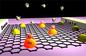 Decorating the surface of graphene with gold nanoparticles results in a more sensitive and versatile material for gas detection.
Feb 15th, 2012
Read more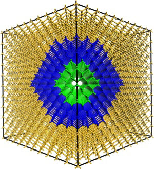 Scientists have performed first-principle calculations to simulate the properties of silicon nanowires with diameters of up to 7.3 nanometers.
Feb 15th, 2012
Read moreIn a boon for the local solar industry, a team of researchers from Swinburne University of Technology and Suntech Power Holdings have developed the world's most efficient broadband nanoplasmonic solar cells.
Feb 15th, 2012
Read more Arizona State University researchers are finding ways to improve infrared photodetector technology that is critical to national defense and security systems, as well as used increasingly in commercial applications and consumer products.
Feb 14th, 2012
Read moreThe new findings indicate that graphene produced using chemical vapor deposition could be a vital alternative for nanomechanical sensor applications.
Feb 14th, 2012
Read more Carbon nanotubes and graphene consist of just a couple of layers of carbon atoms, but they are lighter than aluminium, stronger than steel and can bend like spring-coils. Physicist Niklas Lindahl at the University of Gothenburg, Sweden, has been studying the unique properties of the materials, which in future may result in improved electronics and light, strong material.
Feb 14th, 2012
Read moreAs a result of a joint intensive work of several groups from five different countries, including Basque Country, a new wide class of topological insulators - materials that are insulators in the bulk but conductors at the surface - with technologically very promising properties has been discovered.
Feb 14th, 2012
Read more Using this technique, it is possible to drastically change the electrical behaviour of metals and even to give semiconductors magnetic properties.
Feb 14th, 2012
Read more By reversing the scale of nanotechnology to the realm of human experience, an artist and a scientist create a sublime reversal of space-time.
Feb 14th, 2012
Read moreForschungsarbeiten zu innovativen Beschichtungsmoeglichkeiten fuer Werkzeuge muenden in drei Patentanmeldungen.
Feb 14th, 2012
Read more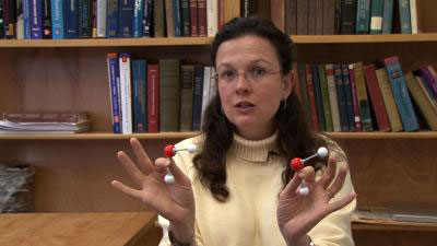 The technology that Google uses to analyze trillions of Web pages is being brought to bear on the way molecules are shaped and organized. A researcher has adapted Google's PageRank software to create moleculaRnetworks, which scientists can use to determine molecular shapes and chemical reactions without the expense, logistics and occasional danger of lab experiments.
Feb 13th, 2012
Read moreEPA and NSF grants funding research to develop more effective treatment technologies.
Feb 13th, 2012
Read morePI is the first nano/micropositioning company to offer its own informative, (mostly) non-commercial app for portable devices like the iPhone, iPad and Android phones and tablets.
Feb 13th, 2012
Read moreThe theme of this year's World Congress on Brain, Spinal Cord Mapping, and Image Guided Therapy is "Nano-Bio-Electronics", which focuses on the integration of nanotechnology, stem cell research, and biomedical engineering, and imaging of the brain and spinal cord to make progress in the fight against neurological diseases.
Feb 13th, 2012
Read more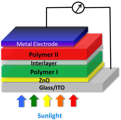 Researchers at the UCLA Henry Samueli School of Engineering and Applied Science and UCLA's California Nanosystems Institute report that they have significantly enhanced polymer solar cells' performance by building a device with a new "tandem" structure that combines multiple cells with different absorption bands. The device had a certified power-conversion efficiency of 8.62 percent and set a world record in July 2011.
Feb 13th, 2012
Read more Subscribe to our Nanotechnology News feed