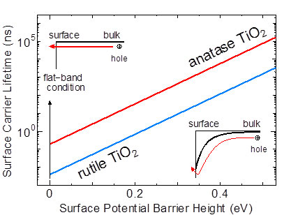
 Researchers have discovered through the in situ observation of the behavior of photoexcited carriers on the surface of a titanium dioxide crystal used as a photocatalyst that the carrier (electron and positive hole) lifetime on the crystal surface is an important factor to determine the catalytic activity.
Feb 18th, 2015
Read more
 A computational technique reveals how tiny pillars affect the condensation of vapor onto a surface.
Feb 18th, 2015
Read more
 Depositing different materials on top of bulk silicon wafers enables three-dimensional opto-electric integration.
Feb 18th, 2015
Read more
 Researchers worked out new chemistry for a broad class of compositions relevant to technologically important semiconductors.
Feb 17th, 2015
Read more
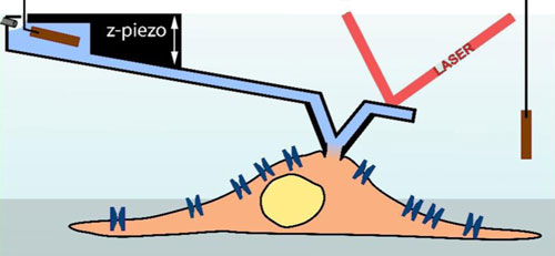 For the first time, scientists have succeeded in recording the current in membrane channels of contracting cardiac cells. To do this, the scientists combined an atomic force microscope with a widely used method for measuring electrical signals in cells.
Feb 17th, 2015
Read more
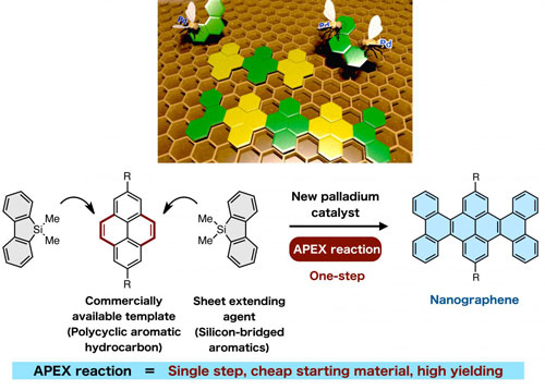 Precisely controlled synthesis of structurally uniform carbon sheets could advance graphene materials science.
Feb 17th, 2015
Read more
 Researchers have developed a unique single-step process to achieve three-dimensional (3D) texturing of graphene and graphite. Using a commercially available thermally activated shape-memory polymer substrate, this 3D texturing, or 'crumpling', allows for increased surface area and opens the doors to expanded capabilities for electronics and biomaterials.
Feb 17th, 2015
Read more
 Measurements have shown how spin filters forming within magnetic sandwiches influence tunnel magnetoresistance - results that can help in designing spintronic components.
Feb 17th, 2015
Read more
 Researchers are exploring new materials that could yield higher computational speeds and lower power consumption, even in harsh environments.
Feb 17th, 2015
Read more
 Scientists are pioneering the use of nanomaterials in compact, sensitive, fast, low-cost terahertz detectors with potential in applications such as biomedical diagnostics, airport security screening and high data-rate wireless communication.
Feb 17th, 2015
Read more
 The latest 'Thematic Issue' publication explores recent developments in nanomaterials research, and possibilities for safe, practical and resource-efficient applications.
Feb 17th, 2015
Read more
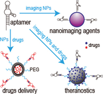 To construct ligand-directed 'active targeting' nanobased delivery systems, aptamer-equipped nanomedicines have been tested for in vitro diagnosis, in vivo imaging, targeted cancer therapy, theranostic approaches, sub-cellular molecule detection, food safety, and environmental monitoring.
Feb 17th, 2015
Read more
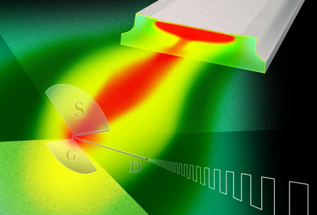
Researchers obtain conductivity values for stroncium iridate 250 times higher than in normal conditions, just pressing with nanometric needles. The results where obtained thanks to the use of the atomic force microscope (AFM) showing that the material could become a good candidate for future applications in sensors and electronics.
Feb 17th, 2015
Read more
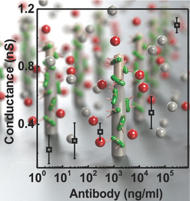 Scientists in Australia propose a label-free electrochemical immunosensor based on functionalized vertical nanowire by means of a current patch clamp amplifi er which has not been previously reported.
Feb 17th, 2015
Read more
 Researchers have made an advance in manufacturing molybdenum disulfide. By growing flakes of the material around 'seeds' of molybdenum oxide, they have made it easier to control the size, thickness and location of the material.
Feb 17th, 2015
Read more
 Molecular beam epitaxy systems enables scientists to control the properties of new crystals with exquisite precision, right down to the atomic level. They can grow nanomaterials with features just a few billionths of a meter across, and even control how many electrons they have inside them.
Feb 17th, 2015
Read more
 Subscribe to our Nanotechnology News feed