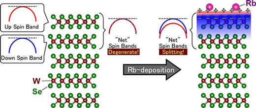
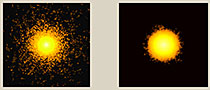
 To understand how a TMD semiconductor behaves inside a device, researchers investigated the effects of sub-monolayer deposition of alkali atoms at the surface of the semiconductor tungsten selenide. These deposited atoms mimics the electric field effects that a semiconductor would experience inside a transistor, while allowing researchers to directly analyse the electronic structure by a state of the art spectroscopic technique.
Oct 5th, 2015
Read more
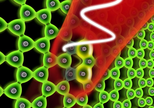 Scientists have made simulations of the processes that happen when a layer of carbon atoms is irradiated with strong laser light.
Oct 5th, 2015
Read more
 Breakthrough could literally reshape solar cells and electronic devices.
Oct 2nd, 2015
Read more
 New computational approach allows researchers to design cellulose nanocomposites with optimal properties.
Oct 2nd, 2015
Read more
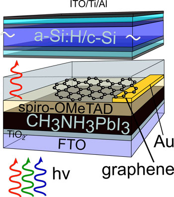 Researchers develop elegant process for coating fragile perovskite layers with graphene for the first time. Subsequent measurements show that the graphene layer is an ideal front contact in several respects.
Oct 2nd, 2015
Read more
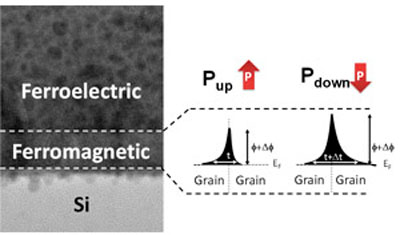 The choice for energy-efficient technologies is not a matter of price choice but it is slowly turning into a matter of heat. A recent work suggests devices fabricated directly on Silicon with magnetic tunnel junctions governed by electric pulses, which means without current and minimizing the problem of overheating.
Oct 2nd, 2015
Read more
Scientists have developed a technology for contactless deposition of liquids at nanoscale. In doing so, they make use of an electric field. Their technology will lead to new 3D-applications and can be of great value to, for example, cell research, nano-lithography and printable electronics.
Oct 2nd, 2015
Read more
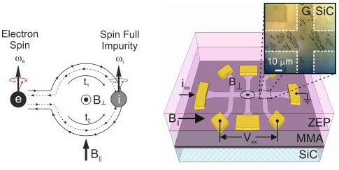 New research shows that applying a moderate in-plane magnetic field increases spin lifetime of electrons in graphene. The results of this work have profound implications for graphene's use as post-CMOS platform in spintronics, and make an important contribution to the understanding of physics of 2D materials.
Oct 2nd, 2015
Read more
 Researchers have arrived at how what is known as time-reversal symmetry can break in one class of superconducting material.
Oct 2nd, 2015
Read more
 Researchers for the first time have applied a modern theory of heat transport in experiments with semiconductors used in computers and lasers, with implications for the design of devices that convert waste heat into electricity and the control of overheating in miniaturized and high-speed electronic components.
Oct 1st, 2015
Read more
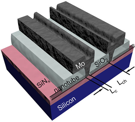 IBM Research today announced a major engineering breakthrough that could accelerate carbon nanotubes replacing silicon transistors to power future computing technologies.
Oct 1st, 2015
Read more
Chemists have developed novel porous materials called 'covalent organic frameworks', which provide a basis for the design of polymeric photocatalysts with tunable physical, chemical and electronic properties.
Oct 1st, 2015
Read more
The revolution of computational materials design is in the making, and the U.S. Department of Energy (DOE) has taken a firm step toward achieving it by creating the Midwest Integrated Center for Computational Materials (MICCoM) at DOE's Argonne National Laboratory.
Oct 1st, 2015
Read more
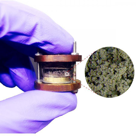 Researchers find that heat can break down the damaging branch-like structures that grow inside batteries, which may possibly be used to extend battery lifetimes.
Oct 1st, 2015
Read more
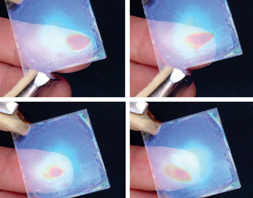
Scientists have worked out an entirely new way to rejuvenate smart windows which have started to show signs of age. The study may open the way to other areas of application.
Oct 1st, 2015
Read more
 Researchers have developed nanostructures that change their electrical and even their optical properties as soon as a finger comes anywhere near them.
Oct 1st, 2015
Read more
 Subscribe to our Nanotechnology News feed