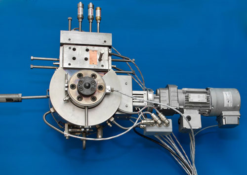
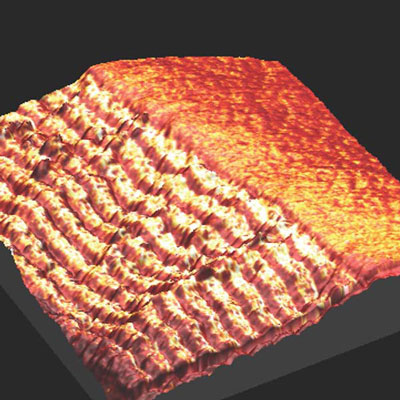
 Nanoparticle additives can make plastics scratch and flame proof, or give them antibacterial properties. For this to work, the particle distribution within the plastic compound must be absolutely correct. A new device is now able to test the distribution in real time.
Nov 4th, 2013
Read more
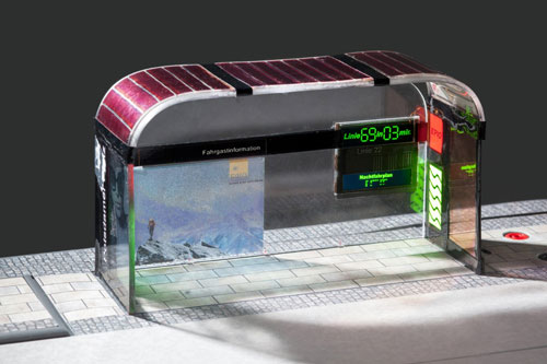 Flickering fa�ades, curved monitors, flashing clothing, fluorescent wallpaper, flexible solar cells - and all printable. This is no make-believe vision of the future; it will soon be possible using a new printing process for organic light-emitting diodes.
Nov 4th, 2013
Read more
The European FP7 Project NanoDiode has officially unveiled its website. Visitors will be able to find the latest information on what activities will be being done by the project around the EU, what publications are considered vital to an understanding, and betterment, of nanotechnology dissemination activities, and see how NanoDiode aims to inspire, educate, co-create and engage with society on nanotechnologies.
Nov 4th, 2013
Read more
An international team of researchers has used pioneering electron microscopy techniques to discover an important mechanism behind the reaction of metallic nanoparticles with the environment. Crucially, the research shows that oxidation of metals - the process that describes, for example, how iron reacts with oxygen, in the presence of water, to form rust - proceeds much more rapidly in nanoparticles than at the macroscopic scale.
Nov 3rd, 2013
Read more
 Research from MIT shows carbon nanotubes that detect nitric oxide can be implanted under the skin for more than a year.
Nov 3rd, 2013
Read more
 First-of-its-kind, brain-inspired device looks toward highly efficient and fast parallel computing networks.
Nov 1st, 2013
Read more
The Symposium will take place on 6-7 November, and the session topics are: Nano Imaging, Manipulation and Diagnostics; Nanoparticles and Nanotherapies; Nanomaterials in Health and Medicine (including Nanotoxicology); and Synthetic Biology.
Nov 1st, 2013
Read more
The NanoSafety Cluster is an EC initiative to maximise the synergies between the past, ongoing and future FP7 nanosafety projects. Each of these projects addresses key aspects of nanosafety, including toxicology, ecotoxicology, exposure assessment, risk assessment, standardisation, and mechanisms of interaction.
Nov 1st, 2013
Read more
Nanotechnology may provide new strategies for regenerative medicine, including better tools to improve or restore damaged tissues, according to a review paper by Taiwanese researchers.
Nov 1st, 2013
Read more
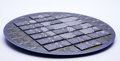 Imec, a world-leading nanoelectronics research center and JSR, a leading materials company, announce that they have successfully used JSR's innovative PA (Photo-patternable Adhesive) material for wafer-scale processing of lab-on-chip devices.
Nov 1st, 2013
Read more
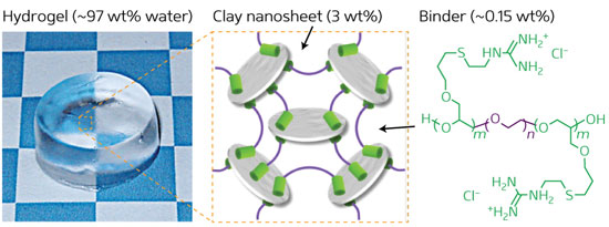 Mechanically tough hydrogels that repair themselves within seconds are now easier to manufacture thanks to novel polymer binding agents.
Nov 1st, 2013
Read more
Nanoscale images may provide 'hole' story on pore-making antibiotic peptides
Oct 31st, 2013
Read more
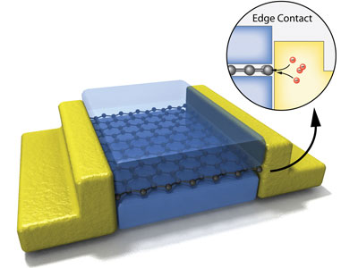 Columbia Engineering researchers have experimentally demonstrated for the first time that it is possible to electrically contact an atomically thin two-dimensional material only along its one-dimensional edge, rather than contacting it from the top, which has been the conventional approach. With this new contact architecture, they have developed a new assembly technique for layered materials that prevents contamination at the interfaces, and, using graphene as the model 2D material, show that these two methods in combination result in the cleanest graphene yet realized.
Oct 31st, 2013
Read more
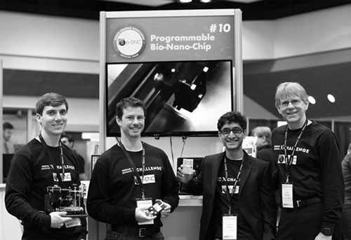 The McDevitt Research Group, a medical micro device group committed to improving the speed, accuracy and affordability of global disease diagnosis, announces the p-BNC, the Programmable Bio-Nano-Chip system.
Oct 31st, 2013
Read more
 A new class of materials developed at the University of Arkansas may influence the next generation of nanotechnology devices, in which integrated circuits are composed of many layers of dissimilar materials.
Oct 31st, 2013
Read more
Researchers at Case Western Reserve University have received two grants totaling nearly $1.7 million to build nanoparticles that seek and destroy metastases too small to be detected with current technologies.
Oct 31st, 2013
Read more
 Subscribe to our Nanotechnology News feed