| Sep 03, 2024 | |
Novel photodetector integrates event sensing and memory for optical processing |
|
| (Nanowerk Spotlight) Optical information processing is a critical technology for applications ranging from machine vision to high-speed optical communication. However, current photodetection systems face significant limitations in processing complex, dynamic optical signals efficiently. Traditional multi-pixel photodetector arrays generate excessive data during dynamic events, leading to high energy consumption and processing inefficiencies. Meanwhile, event-based neuromorphic sensors, which detect changes in light intensity rather than capturing static frames, are limited by their reliance on sequential data input and external processing. | |
| These limitations have spurred research into more advanced optical sensing technologies that can handle high-dimensional spatiotemporal data with lower latency and power consumption. A key challenge has been developing sensors capable of real-time, parallel data processing at a nearly single-pixel scale. This capability is crucial for applications requiring rapid capture and analysis of transient optical phenomena. | |
| Recent advances in materials science and semiconductor device physics have opened new possibilities for addressing these challenges. In particular, the development of wide-bandgap semiconductors and novel device architectures has enabled the creation of photodetectors with unique optoelectronic properties. These advances set the stage for innovative approaches to optical sensing that can potentially overcome the limitations of current technologies. | |
| One promising direction is the integration of sensing and processing capabilities within the same device, a concept known as "in-sensor processing." This approach aims to reduce the need for external computing resources and enable more efficient handling of complex optical signals. However, implementing in-sensor processing for spatiotemporal optical information has remained a significant technical challenge. | |
| Against this backdrop, researchers have been exploring new device designs that can combine multiple functionalities, such as event detection, short-term memory, and parallel data processing, within a single photoactive element. These efforts aim to create more compact, energy-efficient, and capable optical sensors that can better meet the demands of advanced imaging and sensing applications. | |
| A team of researchers at Ajou University in Korea has now reported a significant advance in this field. In a paper published in Advanced Materials ("A Single-Pixel Event Photoactive Device for Real-Time, In-Sensor Spatiotemporal Optical Information Processing"), they describe the development of a novel single-pixel event photoactive device that integrates spatiotemporal event sensing with inherent short-term memory capabilities. This combination of event sensing and memory within a single device is unprecedented and represents a major innovation in optical information processing technology. By merging these two functionalities, the device eliminates the need for external computing resources for memory storage, enabling more compact and energy-efficient designs that are well-suited for real-time applications across various technological domains. | |
| The researchers' work focuses on a carrier-selective, position-sensitive planar photoactive device based on a metal-oxide-semiconductor (MOS) structure. The device utilizes gallium oxide (Ga2O3) as a carrier-selective layer deposited on p-type silicon, creating a unique band alignment that enables both neuromorphic sensing and memory functionalities. | |
 |
|
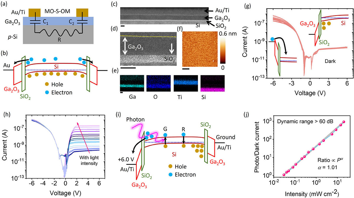
| Device structure and photoresponse characteristics of a Ga2O3/Si-based photodetector. a) Schematic diagram of the planar metal-oxidesemiconductor (MOS) structure with Ga2O3 and Si, indicating capacitors C1 and C2 and resistance R. b) Band diagram showing potential barriers and charge carrier movement. c) Cross-sectional transmission electron microscopy (TEM) image of the device layers. d) High-resolution TEM image highlighting the interfaces between Ga2O3/SiO2 and Si. e) Energy-dispersive X-ray spectroscopy (EDX) mapping showing the distribution of Ga, O, Ti, and Si elements. f) Atomic force microscopy (AFM) image of the surface. The scale bar for (c) is 2 nm, (d) 4 nm, (e) 2 nm, and (f) 1 μm, respectively. g) I–V characteristics of the device under dark conditions. The top and bottom insets show the band alignment with positive and negative bias at Au/Ga2O3/Si, respectively. h) Photoresponse I–V curves at different light intensities showing the sensitivity to light. i) Simplified representation of the charge separation and photocurrent generation under bias. j) Log-log plot of the photo-to-dark current ratio versus light intensity. (Image: Reproduced with permission by Wiley-VCH Verlag) (click on image to enlarge) | |
| This innovative device design allows for in-sensor spatiotemporal parallel optical information processing, efficiently managing multi-bit data simultaneously. The sensor can process more than 4 bits of data in parallel, with an ultrafast recognition time of approximately 0.4 microseconds for input patterns. Importantly, it achieves this performance with remarkably low energy consumption, using only 25 femtojoules per object classification. | |
| The device's functionality is based on its ability to efficiently collect one type of charge carrier, creating a mechanism for both spike generation in response to sudden changes in light intensity and short-term memory effects. The short-term memory capability is achieved through the gradual discharge of charges in the device's capacitive structure. When light illumination changes, it alters the effective carrier density in the absorbing layer, leading to an instant change in the effective applied voltage. This results in photocurrent spikes for sudden light intensity changes, while the gradual discharge of the capacitors mimics short-term memory. | |
| In their experiments, the researchers demonstrated the device's capability to detect changes in its optical environment. They showed that by adjusting the operating speed from continuous to pulsed light illumination, the sensor array can detect both the trajectories and absolute positions of events, offering in-sensor optical flow detection. The device's response was measured under specific conditions, including voltage ranges of ±6.0 V and light intensities up to 20 mW cm-2. | |
| The team's work also explored the device's potential for more complex optical information processing tasks. They showed that the sensor could perform true multi-bit parallel processing of optical data based on illumination sequences, offering a more efficient and direct method for managing complex optical signals. This capability sidesteps the limitations of traditional sensor arrays and modulation techniques. | |
| The implications of this research are substantial, though it's important to note that challenges remain in scaling up the technology for practical applications. The development of a single-pixel event photoactive device with integrated memory and parallel processing capabilities could lead to more efficient optical sensing systems for a range of applications, including advanced machine vision systems and high-speed optical communication networks. However, further optimization and engineering work will be necessary to address scaling challenges and integrate the technology into larger systems. | |
| Moreover, the ultra-low energy consumption of the device points to its potential for use in energy-constrained applications, such as in portable or wearable devices, or in large-scale sensor networks where power efficiency is crucial. | |
| This research marks an important step forward in the field of optical information processing, demonstrating a novel approach that combines multiple advanced functionalities in a single, efficient device. As the technology develops further, it could play a crucial role in enabling the next generation of intelligent optical sensing and processing systems, though the path from laboratory demonstration to practical implementation will require further research and development. | |
 By
Michael
Berger
– Michael is author of three books by the Royal Society of Chemistry:
Nano-Society: Pushing the Boundaries of Technology,
Nanotechnology: The Future is Tiny, and
Nanoengineering: The Skills and Tools Making Technology Invisible
Copyright ©
Nanowerk LLC
By
Michael
Berger
– Michael is author of three books by the Royal Society of Chemistry:
Nano-Society: Pushing the Boundaries of Technology,
Nanotechnology: The Future is Tiny, and
Nanoengineering: The Skills and Tools Making Technology Invisible
Copyright ©
Nanowerk LLC
|
|
|
Become a Spotlight guest author! Join our large and growing group of guest contributors. Have you just published a scientific paper or have other exciting developments to share with the nanotechnology community? Here is how to publish on nanowerk.com. |
|