| Aug 05, 2024 | |
New 2D material junctions power themselves for infrared imaging |
|
| (Nanowerk Spotlight) The miniaturization of electronic devices has driven remarkable technological progress over the past several decades. As components have shrunk to nanoscale dimensions, researchers have explored novel materials and structures to overcome fundamental physical limitations and enable new functionalities. Two-dimensional (2D) materials - atomically thin layers that can be stacked and combined in various ways - have emerged as a promising platform for next-generation electronics and optoelectronics. | |
| These ultra-thin materials exhibit unique quantum and electronic properties not found in conventional bulk materials. Their atomic thinness allows precise control over their structures and properties through techniques like layer engineering. Additionally, different 2D materials can be combined into heterostructures held together by weak van der Waals forces between layers. This enables the creation of atomically sharp interfaces without the lattice matching constraints of traditional semiconductor heterostructures. | |
| Despite their potential, integrating 2D materials into practical devices has remained challenging. Fabrication processes often introduce defects and contamination at material interfaces, degrading performance. Additionally, producing uniform, large-area 2D films suitable for commercial applications has proven difficult. Researchers have long sought methods to overcome these hurdles and harness the unique capabilities of 2D materials for real-world electronic and optoelectronic devices. | |
| A new study published in Advanced Materials ("Integrated Pristine van der Waals Homojunctions for Self-Powered Image Sensors") presents a promising approach to fabricating high-quality devices from 2D materials. The research team, led by scientists from The Hong Kong University of Science and Technology and The Hong Kong Polytechnic University, developed a method to create pristine van der Waals homojunctions from the 2D material molybdenum ditelluride (MoTe2). Unlike typical semiconductor junctions made from different materials, these homojunctions consist of a single material with regions of different thickness. This approach eliminates issues associated with lattice mismatch and interface defects in conventional heterojunctions. | |
 |
|
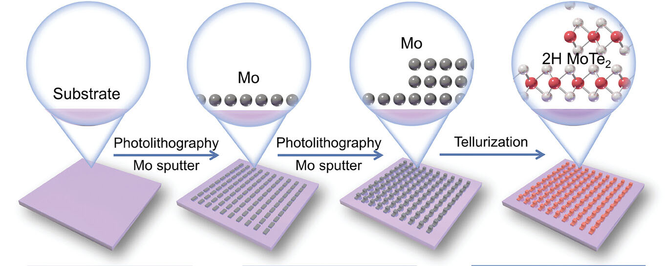
| Schematic of the fabrication processes of patterned 2H-MoTe2 homojunction. (Image: Adoapted from DOI:10.1002/adma.202404013, CC BY) | |
| The researchers used a layer engineering technique to synthesize MoTe2 films with controlled thickness variations. They first deposited patterned molybdenum precursor films of different thicknesses on a sapphire substrate using photolithography and sputtering. These precursor patterns were then converted into 2H-phase MoTe2 through a chemical vapor deposition process called tellurization. | |
| Detailed characterization confirmed the high quality and pristine nature of the resulting MoTe2 homojunctions. Transmission electron microscopy revealed atomically sharp interfaces between regions of different thickness, with no signs of defects or disorder. The electronic properties of the MoTe2 films were found to vary with thickness due to quantum confinement effects. This allowed the researchers to create built-in electric fields at homojunction boundaries by engineering the thickness difference between adjacent regions. | |
| Leveraging these built-in fields, the team demonstrated self-powered photodetectors operating without any external bias voltage. The thickness-engineered MoTe2 homojunctions were able to efficiently separate and collect photogenerated charge carriers, producing electrical signals in response to both visible and near-infrared light illumination. Notably, the photodetectors exhibited broadband sensitivity from 520 nm to 1060 nm wavelengths. | |
| To showcase the scalability and integration potential of their approach, the researchers fabricated an image sensor array consisting of 10x10 MoTe2 homojunction photodetector pixels. This proof-of-concept device was able to capture low-resolution images using near-infrared illumination without any external power supply. The consistent performance across pixels highlights the uniformity achievable with the layer engineering synthesis method. | |
 |
|
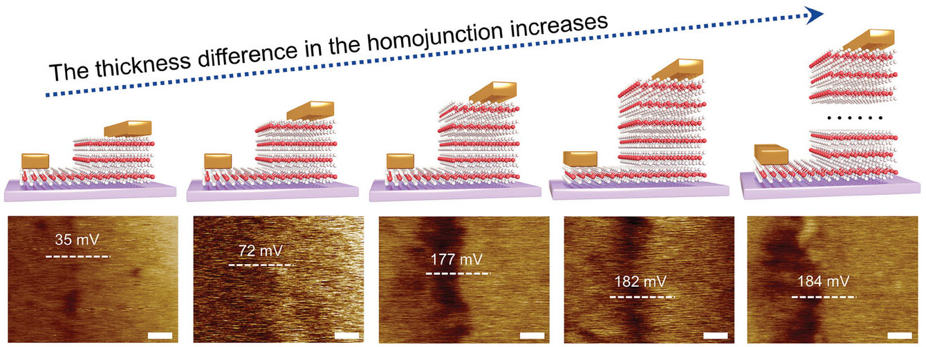
| 2H-MoTe2 homojunctions with thickness difference increasing. a) Schematic diagram of the 2H-MoTe2 homojunction device with thickness difference between thick region and thin region increasing. b) The Kelvin probe force microscopy (KPFM) mapping of the 2H-MoTe2 homojunction with thickness difference increasing. The scale bar is 1 nm.(Image: Adoapted from DOI:10.1002/adma.202404013, CC BY) | |
| The work represents a significant advance in fabricating high-quality optoelectronic devices from 2D materials. By creating pristine homojunctions through thickness engineering, the researchers avoided many of the interface issues that have limited the performance of previous 2D material heterostructure devices. The ability to precisely control the electronic properties and built-in fields in these structures enables new device designs not possible with conventional materials. | |
| The self-powered operation of the MoTe2 homojunction photodetectors is particularly noteworthy. Most semiconductor photodetectors require an external voltage bias to separate and collect photogenerated carriers. The built-in fields in these engineered homojunctions allow efficient charge separation without any applied voltage. This could enable ultralow-power optical sensing and imaging systems for applications like wearable electronics, Internet of Things devices, and remote environmental monitoring. | |
| The broadband sensitivity of the MoTe2 devices, spanning visible to near-infrared wavelengths, is also advantageous for many sensing applications. Near-infrared detection is important for night vision, optical communications, and biomedical imaging. The ability to detect both visible and near-infrared light with a single material system could simplify and reduce the cost of multi-spectral imaging systems. | |
| While the current work focused on MoTe2, the layer engineering approach could likely be extended to other 2D materials and combinations. This opens up possibilities for creating a diverse array of pristine homojunction and heterojunction devices with precisely tuned properties. The compatibility of the fabrication process with standard semiconductor manufacturing techniques is also promising for potential commercial applications. | |
| However, several challenges remain before such devices can be practically implemented. The current synthesis method is limited to relatively small substrate sizes. Scaling up to wafer-scale production while maintaining material quality and uniformity will be crucial. Additionally, while the 10x10 pixel array demonstrates basic imaging capabilities, much higher pixel densities would be needed for most real-world applications. Optimizing device architectures and readout circuitry to enable larger, higher-resolution arrays is an important next step. | |
| Long-term stability and reliability of 2D material devices in various operating environments also needs further study. Encapsulation techniques may be necessary to protect the atomically thin layers from degradation. Integration with conventional electronic components and packaging solutions compatible with 2D materials will likewise require additional development. | |
| Despite these challenges, the pristine van der Waals homojunctions demonstrated in this work represent an important step toward practical optoelectronic devices based on 2D materials. The ability to create high-quality junctions with built-in fields through thickness engineering opens new possibilities for device designs. | |
 By
Michael
Berger
– Michael is author of three books by the Royal Society of Chemistry:
Nano-Society: Pushing the Boundaries of Technology,
Nanotechnology: The Future is Tiny, and
Nanoengineering: The Skills and Tools Making Technology Invisible
Copyright ©
Nanowerk LLC
By
Michael
Berger
– Michael is author of three books by the Royal Society of Chemistry:
Nano-Society: Pushing the Boundaries of Technology,
Nanotechnology: The Future is Tiny, and
Nanoengineering: The Skills and Tools Making Technology Invisible
Copyright ©
Nanowerk LLC
|
|
|
Become a Spotlight guest author! Join our large and growing group of guest contributors. Have you just published a scientific paper or have other exciting developments to share with the nanotechnology community? Here is how to publish on nanowerk.com. |
|