| Aug 02, 2024 | |
Two-atom-thick boron sheets rival silicon in race for smaller electronics |
|
| (Nanowerk Spotlight) The field of two-dimensional materials has seen remarkable progress since the isolation of graphene in 2004. This atomically thin form of carbon sparked intense research into other potential 2D materials with unique and useful properties. While graphene's exceptional electrical conductivity and strength garnered significant attention, its lack of a bandgap limited its applicability in semiconductor devices. This drove scientists to explore alternative 2D materials that could potentially combine graphene's desirable traits with semiconductor behavior. | |
| One such material that has attracted considerable interest is borophene - a single-atom-thick sheet of boron atoms. First theoretically predicted in the 1990s, borophene remained elusive experimentally for decades due to the challenges of synthesizing such an unstable structure. Unlike graphene, which can be mechanically exfoliated from bulk graphite, boron does not naturally form layered structures. This necessitated the development of specialized synthesis techniques to create borophene. | |
| It wasn't until 2015 that researchers successfully fabricated the first borophene sheets on silver substrates using molecular beam epitaxy. This breakthrough opened up new avenues for exploring borophene's properties and potential applications. Initial studies revealed that borophene exhibited metallic behavior, unlike the semiconducting nature of bulk boron. While this metallic character was intriguing for certain applications, it still left a gap in the search for 2D semiconductors that could rival silicon in electronic devices. | |
| The quest for 2D semiconductors with properties comparable to silicon has been driven by the increasing demand for miniaturization in electronics. As traditional silicon-based devices approach their physical limits, there is a growing need for ultra-thin materials that can maintain or improve upon silicon's electronic properties. This has led researchers to investigate various 2D materials, including transition metal dichalcogenides like molybdenum disulfide, as well as elemental 2D materials like phosphorene. | |
| Against this backdrop, a recent study published in Advanced Functional Materials ("Bilayer Borophenes Exhibit Silicon-Like Bandgap and Carrier Mobilities") presents a significant development in the field of 2D materials. Researchers have discovered that bilayer borophene, consisting of two stacked sheets of boron atoms, exhibits semiconductor properties remarkably similar to those of silicon. This finding represents a potential breakthrough in the search for 2D semiconductors that could maintain the miniaturization trend in electronics. | |
| The study focused on a specific structure of bilayer borophene known as the v1/12 bilayer, which is composed of two v1/12 boron sheets stacked in an AB configuration. Through extensive computational modeling and first-principles calculations, the researchers investigated the electronic and optical properties of this bilayer structure. | |
 |
|
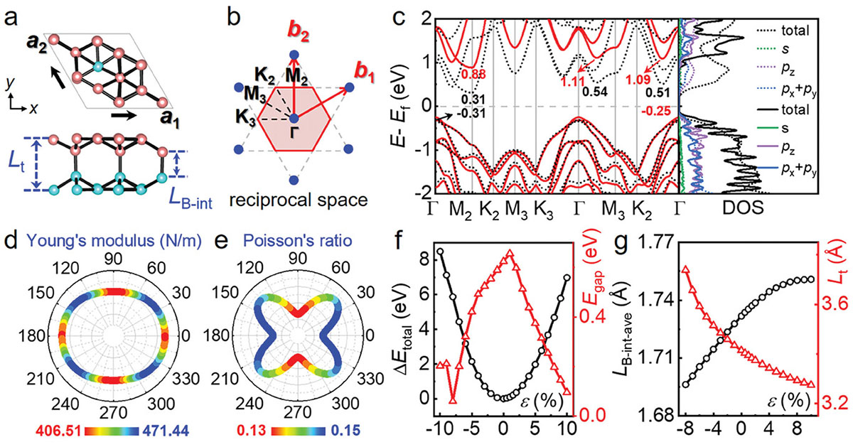
| Structure and electronic properties of the v1/12 bilayer. a) Top and side views of the v1/12 bilayer, with top and bottom boron sheets highlighted in pink and blue, respectively. b) Basis vectors for the rhombic unit cell in real space (a1, a2) and reciprocal space (b1, b2), as well as high-symmetry points in the first Brillouin zone of the v1/12 bilayer. c) Band structure and the corresponding density of states (DOS) of the v1/12 bilayer calculated using the PBE (dotted lines) and HSE (solid lines) methods. e) Young’s modulus and f) Poisson’s ratio of the v1/12 bilayer. (f) Total energy (Etotal, black circle) and band gap (Egap, red triangle) of the v1/12 bilayer as functions of the biaxial strain (𝜖). The pristine v1/12 bilayer is set as the reference point. g) Average interlayer B─B bond length (LB-int-ave) and thickness (Lt) of the v1/12 bilayer as functions of the biaxial strain, with corresponding graphical representations in (a). (Image: Reproduced with permission by Wiley-VCH Verlag) (click on image to enlarge) | |
| One of the most striking findings is that the v1/12 bilayer borophene has a bandgap of 1.13 electron volts (eV), almost identical to that of silicon (1.1 eV). This bandgap is crucial for semiconductor applications, as it determines the energy required for electrons to move from the valence band to the conduction band. The similarity to silicon's bandgap suggests that bilayer borophene could potentially serve as a direct replacement for silicon in certain electronic devices, while offering the advantages of a two-dimensional material. | |
| The researchers delved into the factors that contribute to the opening of this bandgap in bilayer borophene. They found that the stacking mode between the two boron sheets, as well as the density and pattern of interlayer boron-boron bonds, play critical roles in determining the electronic properties. By systematically investigating various configurations of bilayer borophene, they identified specific structures that exhibit semiconducting behavior. | |
| Another crucial parameter for semiconductor performance is carrier mobility, which measures how quickly electrons or holes can move through a material when an electric field is applied. Using advanced computational methods that account for electron-phonon coupling, the researchers calculated the electron mobility of the v1/12 bilayer borophene to be 878.6 cm2 V-1 s-1. This value is remarkably close to the electron mobility of silicon, further highlighting the potential of bilayer borophene as a silicon alternative in nanoelectronics. | |
| The study also revealed that bilayer borophene possesses superior optical properties compared to silicon. In particular, the absorption coefficient of bilayer borophene in the visible light spectrum is significantly higher than that of silicon, with absorption coefficients reaching up to 6% compared to silicon's lower values. This enhanced light absorption could make bilayer borophene an attractive material for optoelectronic applications, such as solar cells or photodetectors. | |
| The researchers conducted a comprehensive analysis of the structural stability and electronic properties of various bilayer borophene configurations. They found that semiconducting bilayer structures demonstrated superior dynamical and thermal stability compared to their metallic counterparts. This stability is crucial for practical applications, as it ensures the material can maintain its desirable properties under typical operating conditions. | |
| One of the intriguing aspects of bilayer borophene revealed by this study is its structural flexibility. The researchers identified potential pathways for structural transitions between different bilayer configurations. These transitions could potentially be induced by external factors such as strain or doping, offering a degree of tunability to the material's properties. | |
| The anisotropic nature of bilayer borophene's properties was also thoroughly investigated. The material exhibits directional dependence in various characteristics, including elastic properties, carrier mobility, and optical absorption. For instance, electron mobility along the bx1 direction can reach up to 1.26 × 104 cm2 V-1 s-1, significantly higher than along the by2 direction. Similarly, the optical absorption coefficient varies with direction, providing potential advantages in applications where directional control of electronic or optical properties is desired. | |
| While the study primarily relied on computational methods, the researchers validated their approach by comparing their results with experimental data where available. They also employed multiple computational techniques to cross-verify their findings, enhancing the reliability of their predictions. | |
| The discovery of semiconductor behavior in bilayer borophene comparable to that of silicon opens up exciting possibilities for the future of nanoelectronics. As traditional silicon-based technologies approach their physical limits, 2D materials like bilayer borophene could potentially enable the continued miniaturization of electronic devices while maintaining or even improving performance. | |
| However, it's important to note that significant challenges remain before bilayer borophene can be practically implemented in electronic devices. The synthesis and large-scale production of high-quality bilayer borophene with precise control over its structure and properties will require further research and development. Additionally, integration with existing semiconductor manufacturing processes and the development of suitable contact materials and device architectures will be necessary steps toward practical applications. | |
 By
Michael
Berger
– Michael is author of three books by the Royal Society of Chemistry:
Nano-Society: Pushing the Boundaries of Technology,
Nanotechnology: The Future is Tiny, and
Nanoengineering: The Skills and Tools Making Technology Invisible
Copyright ©
Nanowerk LLC
By
Michael
Berger
– Michael is author of three books by the Royal Society of Chemistry:
Nano-Society: Pushing the Boundaries of Technology,
Nanotechnology: The Future is Tiny, and
Nanoengineering: The Skills and Tools Making Technology Invisible
Copyright ©
Nanowerk LLC
|
|
|
Become a Spotlight guest author! Join our large and growing group of guest contributors. Have you just published a scientific paper or have other exciting developments to share with the nanotechnology community? Here is how to publish on nanowerk.com. |
|