| Jul 26, 2024 | |
Graphene-quantum dot hybrid enables compact multispectral light detection |
|
| (Nanowerk Spotlight) Light detection across multiple wavelengths underpins numerous technological applications, from environmental monitoring to medical diagnostics. Traditional multispectral photodetectors, however, often rely on bulky components like beam splitters or interferometers, limiting their miniaturization potential. This constraint has long challenged researchers seeking to integrate advanced spectral sensing capabilities into compact devices. | |
| Recent years have seen significant strides in nanomaterials research, particularly in the areas of two-dimensional materials like graphene and zero-dimensional materials like colloidal quantum dots. These materials offer unique properties that make them attractive for next-generation optoelectronic devices. Graphene boasts exceptionally high carrier mobility, while quantum dots provide size-tunable optical properties. Despite their promise, effectively combining these materials to create practical, high-performance devices has remained elusive. | |
| Researchers have now developed an innovative approach to multispectral photodetection by alternating layers of graphene and colloidal quantum dots. This novel architecture, detailed in Advanced Functional Materials ("Intercalated Graphene and Colloidal Quantum Dots for Multispectral Photodetection"), enables probing of photocurrent at various depths within the device structure. By carefully engineering the material stack, the team created photodetectors sensitive to different wavelength bands without additional optical components. | |
| The key innovation lies in using graphene monolayers as independent charge collectors at different depths within a quantum dot absorber layer. Each graphene sheet has dedicated electrical contacts, allowing separate photocurrent measurement for each layer. This multilayer structure distinguishes between spectral bands based on where photocurrent generates within the device, exploiting the wavelength-dependent nature of light absorption depth. | |
 |
|
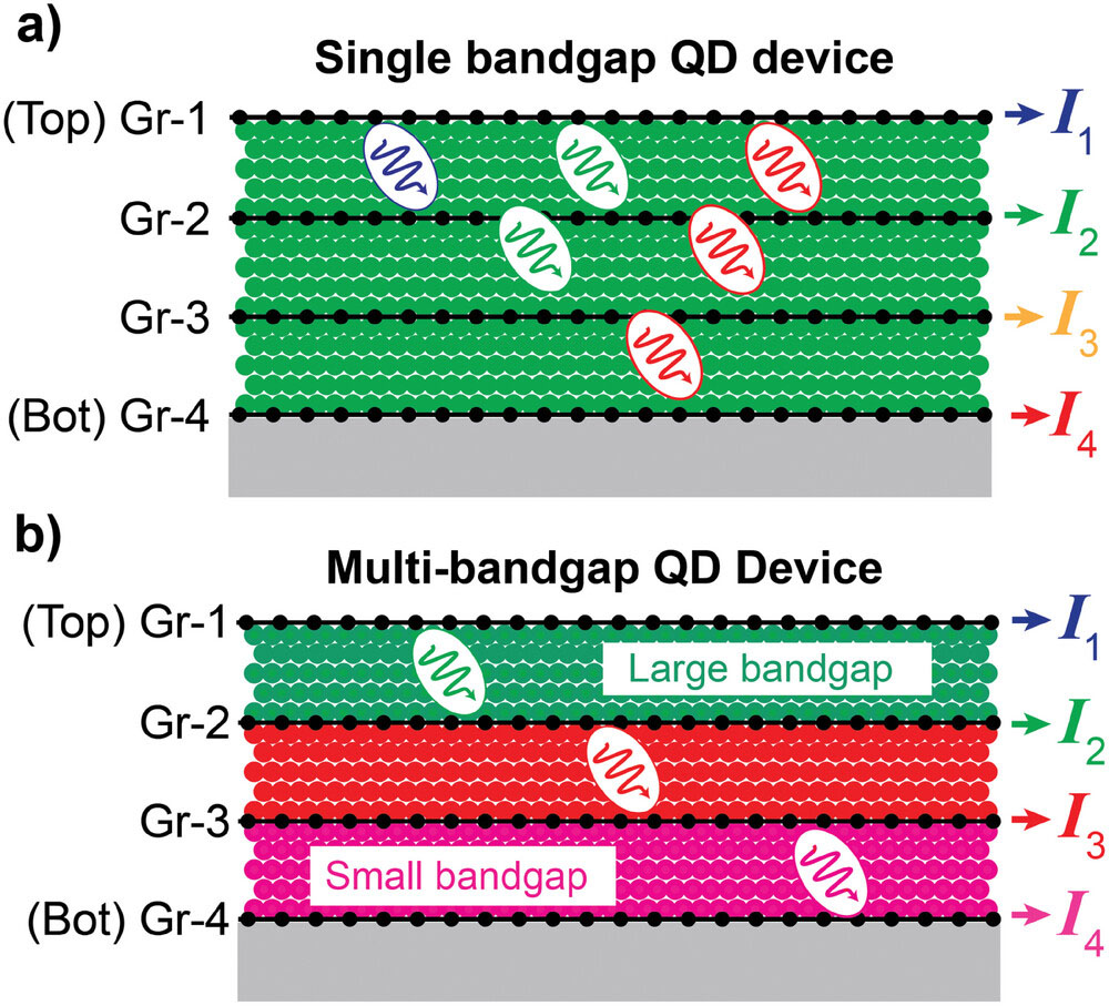
| Device operation principle. Intercalated devices based on sequential stacking of QDs and graphene with independent electrodes to measure the current through each individual graphene monolayer (I1 through I4). QDs act as light absorbers and photocarrier generators. Graphene monolayers serve as independent charge collectors to collect photocarriers generated in adjacent, top and bottom, QD layers. a) Single-Bandgap devices have only one type of PbS QDs. Shorter wavelengths can be detected in the top layers due to the short penetration depth, while longer wavelengths are detected through the entire stack due to the longer penetration depths. b) Multi-Bandgap devices have PbS QDs of different sizes with decreasing bandgap from top to bottom. Short wavelengths are absorbed mainly at the top layers, while long wavelengths are absorbed mainly at bottom layers. (Image: reproduced with permission by Wiley-VCH Verlag) | |
| To demonstrate this approach, the researchers fabricated two device types. The "Single-Bandgap" device used uniform-sized quantum dots throughout, with an absorption peak around 920 nanometers. This device incorporated four graphene layers interspersed with quantum dot layers, measuring photocurrent at four depths. As anticipated, top graphene layers showed stronger responses to shorter wavelengths, while deeper layers were more sensitive to longer-penetrating wavelengths. | |
| To expand spectral range and enhance wavelength discrimination, the team also created "Multi-Bandgap" devices using quantum dots of varying sizes. By decreasing quantum dot bandgaps from top to bottom, they tuned the device's absorption profile. This configuration resulted in short wavelengths absorbing mainly in top layers, while longer wavelengths primarily absorbed in bottom layers. Multi-Bandgap devices demonstrated an expanded spectral response range of 400-1500 nanometers, compared to 400-1200 nanometers for Single-Bandgap devices. | |
| Intriguingly, Multi-Bandgap devices exhibited a negative photoresponse coefficient for longer wavelengths, meaning deeper graphene layers showed stronger responses than top layers for these wavelengths. This unexpected behavior stems from the strategic arrangement of quantum dots with different bandgaps. Larger-bandgap quantum dots near the device top absorb shorter wavelengths, while smaller-bandgap dots at the bottom capture longer wavelengths. This creates an internal wavelength filtering effect. | |
| For infrared wavelengths, photons pass through upper layers with minimal absorption, then encounter smaller-bandgap quantum dots in deeper layers. Here, they generate a stronger photoresponse, resulting in larger photocurrents from deeper graphene layers. This built-in wavelength discrimination mechanism could simplify spectral analysis in the infrared region, potentially eliminating the need for external filters or complex optical components. | |
| This phenomenon not only provides a clear method for distinguishing between different wavelength ranges but also extends the device's effective detection range. It demonstrates how engineered nanomaterial structures can create emergent properties surpassing individual component capabilities, opening new possibilities for compact, multifunctional photodetectors. | |
| The fabrication process, while complex, proves the feasibility of creating intricate nanostructured optoelectronic devices. Combining wet transfer techniques for graphene layers and spin coating for quantum dot layers, along with precise patterning and etching, allowed the team to build devices with up to five graphene and five quantum dot layers. This provides multiple independent channels for spectral detection. | |
 |
|
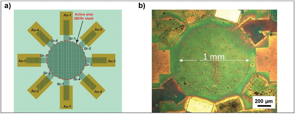
| Device scheme and image. a) Device diagram that shows an array of gold electrodes contacting different graphene layers at different depths in an intercalated Gr/PbS QD stacked film. b) A fabricated device shows the gold electrodes and a central stacked active device with intercalated Gr/PbS QD devices. The central active circular area has a diameter of 1 mm. (Image: reproduced with permission by Wiley-VCH Verlag) | |
| To quantify device performance, the researchers introduced the "photocurrent depth coefficient," which measures normalized photocurrent changes with depth for different wavelengths. This parameter encodes the device's spectral response and could enable wavelength identification and spectral analysis. | |
| While promising, challenges remain before practical implementation. Spectral responses of different graphene layers still overlap significantly, limiting exclusive spectral range assignment to each layer. Improving separation may require further device structure optimization, such as incorporating thicker quantum dot layers or insulating barriers between graphene layers. | |
| The researchers also noted variations in coupling and photocurrent levels between quantum dots and graphene for different dot sizes. This highlights the need for better understanding of charge transfer mechanisms in these hybrid systems and potential improvements in surface chemistry to enhance photocarrier transfer. | |
| Device response times, while suitable for many applications, lag behind some conventional photodetectors. Observed response times ranged from 70-80 milliseconds, with recovery times of 200-300 milliseconds and slower components extending to about 2 seconds. Improving speed may require exploring alternative device geometries or optimizing materials and interfaces. | |
| Despite these challenges, the approach offers several advantages over existing technologies. The compact, thin-film nature of the devices (around 1 micrometer thick) suits them for integration into miniaturized systems. Detecting multiple spectral bands without additional optical components could enable new applications in portable spectroscopy, environmental sensing, and medical diagnostics. | |
| This work opens new avenues for research into hybrid nanomaterial systems for optoelectronics. Combining graphene's unique properties with quantum dots' tunable optical characteristics may lead to a new class of engineered photonic devices surpassing conventional semiconductors' capabilities. | |
| Future research may focus on further expanding the spectral range, potentially into the mid-wave infrared region by incorporating different quantum dot types or other nanomaterials. Improving fabrication processes to enhance reliability and yield will be crucial for practical applications. Developing sophisticated data analysis techniques, possibly leveraging machine learning, could extract more information from these multilayer devices' complex spectral responses. | |
| The concept of using intercalated graphene and quantum dot layers for multispectral photodetection marks a significant step toward more compact and versatile light-sensing technologies. As refinement continues, these devices may enable new capabilities in environmental monitoring, food safety, medical diagnostics, and autonomous vehicles. This technology could contribute to the development of more sophisticated, ubiquitous sensing networks, potentially transforming how we interact with and understand our environment through light-based analysis. | |
 By
Michael
Berger
– Michael is author of three books by the Royal Society of Chemistry:
Nano-Society: Pushing the Boundaries of Technology,
Nanotechnology: The Future is Tiny, and
Nanoengineering: The Skills and Tools Making Technology Invisible
Copyright ©
Nanowerk LLC
By
Michael
Berger
– Michael is author of three books by the Royal Society of Chemistry:
Nano-Society: Pushing the Boundaries of Technology,
Nanotechnology: The Future is Tiny, and
Nanoengineering: The Skills and Tools Making Technology Invisible
Copyright ©
Nanowerk LLC
|
|
|
Become a Spotlight guest author! Join our large and growing group of guest contributors. Have you just published a scientific paper or have other exciting developments to share with the nanotechnology community? Here is how to publish on nanowerk.com. |
|