| Jul 08, 2024 | |
New shapes of confined light open doors to advanced optical technologies |
|
| (Nanowerk Spotlight) The manipulation and control of light at the nanoscale has been a longstanding goal in the field of photonics, with far-reaching implications for technologies ranging from telecommunications to quantum computing. Researchers have made significant strides in confining and directing light using various structures, from simple optical fibers to complex photonic crystals. | |
| However, achieving three-dimensional confinement of light in a way that allows for precise control and manipulation has remained a challenging frontier. Previous attempts have often been limited to one or two dimensions or have struggled with issues of light leakage and inefficient coupling between confined light states. | |
| The development of photonic band gap materials in the 1990s offered a promising avenue for three-dimensional light confinement, but realizing practical devices based on these concepts has proven difficult due to fabrication challenges and the need for precise control over structural parameters at the nanoscale. | |
| Recent advances in nanofabrication techniques, particularly in the creation of complex three-dimensional nanostructures, have opened up new possibilities for photonic devices. One particularly intriguing structure is the inverse woodpile photonic crystal, which consists of a lattice of nanoscale pores arranged in a diamond-like configuration within a high-refractive-index material such as silicon. These structures can exhibit a complete photonic band gap, a range of frequencies for which light propagation is forbidden in all directions. | |
| By introducing intentional defects into this structure, researchers have sought to create localized states where light can be trapped and manipulated. This approach draws parallels to the doping of semiconductors in electronics, where intentional impurities create new electronic states within the band gap of the material. | |
| A new study published in Physical Review B ("Symmetries and wave functions of photons confined in three-dimensional photonic band gap superlattices") by researchers from the University of Twente in the Netherlands has made significant progress in understanding and controlling light confinement in three-dimensional photonic band gap superlattices. The team, led by Marek Kozoň and Willem L. Vos, performed a comprehensive computational investigation of optical states in inverse woodpile photonic crystals with periodic defects, creating what they term a "cavity superlattice." | |
 |
|
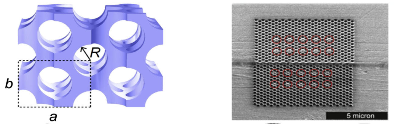
| Figure 1. (Left): Design of the Twente photonic crystal consisting of silicon (blue) with arrays of air pores pointing into the screen and parallel to the screen. (Right) Electron microscopy image of a photonic crystal nanostructure made by the Twente team from silicon (grey). The nanostructure consists of nanometer-sized pores that are etched deep into the silicon with methods developed by COPS, MESA+. The red circles indicate pores that are on purpose made smaller. At the crossings of pairs of smaller pores (inside the structure) cavities occur where the photonic waves form their novel orbitals. (Image: Courtesy of the researchers) | |
| The researchers focused on a specific type of inverse woodpile structure made of silicon, with two perpendicular arrays of nanopores. By altering the radius of certain pores in a periodic pattern, they created a superlattice of optical cavities within the photonic crystal. Using advanced computational techniques, including a novel scaling analysis method, they were able to identify and characterize the optical modes that arise in these structures. | |
| One of the key findings of the study is the identification of what the researchers call "Cartesian light" – optical states that are confined in all three dimensions but can "hop" between adjacent cavities in specific One of the key findings of the study is the identification of what the researchers call "Cartesian light" – optical states that are confined in all three dimensions but can "hop" between adjacent cavities in specific – primarily (x,y,z) – directions, as opposed to traveling in any direction as in free space. This behavior is analogous to the tight-binding model used to describe electrons in solid-state physics, but with some crucial differences. | |
| The team discovered that the symmetries and spatial distributions of these confined optical states, which they term "photonic orbitals," are more varied and complex than those of electronic orbitals in atoms. This difference arises because the photonic states derive from global Bloch states governed by the overall superlattice structure, rather than from localized atomic orbitals. | |
| First author Kozoň explains this distinction to Nanowerk: "In textbook chemistry, the electrons always orbit around the tiny atomic core at the center of the orbital. So an electron orbital's shape cannot deviate much from a perfect sphere. With photons, the orbitals can have whatever wild shape you design by combining different optical materials in designed spatial arrangements." | |
| This realization opens up intriguing possibilities for creating "photonic solid-state matter" with properties that have no direct analog in electronic systems. Physicists Vos and Lagendijk emphasize the potential of this approach: "Given the rich toolbox in nanotechnology, it is much easier to design nifty nanostructures with novel photonic orbitals than it is to modify atoms to realize novel electronic orbitals and chemistry." | |
 |
|
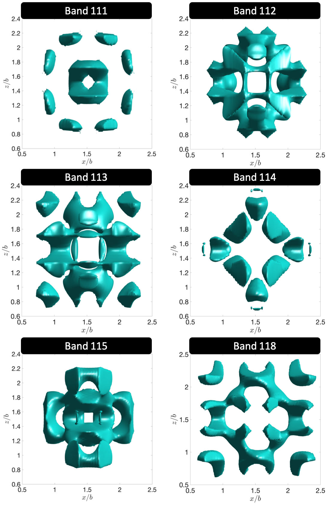
| Figure 2: Several different photonic orbitals that arise within a photonic crystal superlattice as is shown in Figure 1. Increasing band numbers (111, 112, etc.) correspond to increasing photon energies. The photonic orbitals are viewed along the y-axis. While this view seems to suggest a 90° rotational symmetry in the orbitals, this is not the case on 3D inspection. The orbitals reveal rich new shapes and symmetries not found with electronic orbitals in atomic crystals. For instance, the orbitals exhibit mirror symmetries with respect to the 𝑥/𝑏=1.5 and 𝑧/𝑏=1.5 planes, that pass through the axes of each defect pore, and are designed by the researchers. The orbital of band 111 has a high energy density that is favorable for cavity quantum electrodynamics applications. (Image: Courtesy of the researchers) | |
| The researchers conducted a thorough analysis of how the confined optical states depend on the structural parameters of the photonic crystal, particularly the radii of the regular and defect pores. They created "confinement maps" that show which combinations of pore sizes lead to strongly confined optical modes. These maps reveal that there is a minimum difference between the regular and defect pore sizes necessary for three-dimensionally confined states to appear. Additionally, they found that larger pore sizes generally favor the existence of more confined states and lead to higher energy concentrations within the cavities. | |
| One particularly interesting discovery was the identification of pairs of degenerate confined bands with symmetries that match those of the underlying superlattice structure. These states could potentially be used to create novel quantum optical devices or to study fundamental aspects of light-matter interactions in three dimensions. | |
| The study also investigated the enhancement of the local density of optical states (LDOS) within the cavities, which is crucial for applications in cavity quantum electrodynamics. The researchers found that "donor like" superlattices, where the defect pores are smaller than the regular pores, provide greater LDOS enhancement in the air regions of the structure. This configuration could be particularly useful for integrating quantum emitters like quantum dots into the cavities, potentially enabling the creation of three-dimensional networks of strongly coupled optical cavities for quantum information processing applications. | |
| The findings of this study have significant implications for the development of advanced photonic devices. The ability to precisely control and manipulate light in three dimensions could lead to more efficient optical interconnects for computing, enhanced sensors for detecting biological or chemical substances, and novel platforms for studying quantum optical phenomena. The rich symmetries and spatial distributions of the confined optical states might also inspire new approaches to designing metamaterials with unusual optical properties. | |
| The researchers highlight several potential applications for their work, including smart LED lighting, new photonic bits of information controlled with quantum circuits, and sensitive nanosensors. The ability to design and control photonic orbitals with a wide variety of shapes and symmetries opens up new possibilities for tailoring light-matter interactions at the nanoscale. | |
| However, it's important to note that this work is primarily computational, and translating these results into practical devices will require overcoming significant fabrication challenges. Creating inverse woodpile structures with the necessary precision and uniformity at the nanoscale remains difficult, especially for the larger pore sizes that the study found to be most favorable for confinement. | |
| Recently, the Twente team published a preprint ("Observation of light propagation through a three-dimensional cavity superlattice in a 3D photonic band gap") that reports the first fabricated cavity superlattices with the first observations of Cartesian hopping of photons between cavities. | |
| Despite these challenges, the comprehensive understanding of light confinement in three-dimensional photonic band gap superlattices provided by this study represents a significant step forward in the field of nanophotonics. As fabrication techniques continue to improve, the insights gained from this work could guide the development of a new generation of photonic devices that harness the full potential of three-dimensional light confinement, paving the way for advanced optical technologies and quantum photonic systems. | |
 By
Michael
Berger
– Michael is author of three books by the Royal Society of Chemistry:
Nano-Society: Pushing the Boundaries of Technology,
Nanotechnology: The Future is Tiny, and
Nanoengineering: The Skills and Tools Making Technology Invisible
Copyright ©
Nanowerk LLC
By
Michael
Berger
– Michael is author of three books by the Royal Society of Chemistry:
Nano-Society: Pushing the Boundaries of Technology,
Nanotechnology: The Future is Tiny, and
Nanoengineering: The Skills and Tools Making Technology Invisible
Copyright ©
Nanowerk LLC
|
|
|
Become a Spotlight guest author! Join our large and growing group of guest contributors. Have you just published a scientific paper or have other exciting developments to share with the nanotechnology community? Here is how to publish on nanowerk.com. |
|