| Jul 01, 2024 | |
Machine learning uncovers new semiconductors with unique square-octagonal structure |
|
| (Nanowerk Spotlight) The pursuit of novel materials with extraordinary properties has been a driving force in scientific research, propelling advancements across various industries. In recent years, attention has increasingly focused on two-dimensional (2D) materials, inspired by the remarkable success of graphene. Among these, a class of compounds known as Haeckelites has emerged as a promising frontier. Haeckelites, named after the German biologist Ernst Haeckel, are characterized by their unique square-octagonal structure, reminiscent of certain biological forms observed in nature. | |
| The exploration of Haeckelites gained momentum following the experimental synthesis of beryllium oxide (BeO) in this configuration. This achievement sparked interest in the potential of other elements to form similar structures, each with its own set of properties. However, the challenge lies in identifying which combinations of elements could form stable Haeckelite structures and exhibit desirable characteristics for practical applications. | |
 |
|
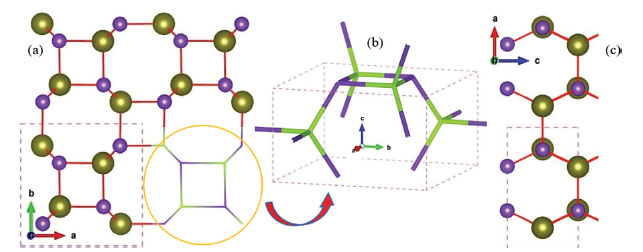
| a) Top view and b) 3D form of unit cell connections and c) side view of 2 × 2 × 1, XY Haeckelite structure. A pink square indicates the primitive unit cell. Because of the symmetry, the (1,0,0) and (0,1,0) directions are the same view. (Reprinted with permission by Wiley-VCH Verlag) | |
| Traditionally, the discovery of new materials has been a time-consuming and resource-intensive process, relying heavily on trial-and-error experimentation. The advent of computational methods has accelerated this process, allowing researchers to screen vast numbers of potential compounds before attempting synthesis in the laboratory. Yet, even with these advancements, the sheer number of possible element combinations remains daunting. | |
| Recent years have seen the integration of machine learning techniques into materials science, offering a powerful tool to predict material properties and guide experimental efforts. This approach has proven particularly valuable in the search for new 2D materials, where the interplay between structure and properties is complex and often counterintuitive. Machine learning models, such as the random forest regressor (RFR) used in this study, have shown exceptional ability to handle complex, non-linear relationships in materials data, making them well-suited for predicting properties like formation energy and bandgap. | |
| Against this backdrop, a team of researchers has undertaken a comprehensive study of Haeckelite structures, aiming to identify new compounds with potential applications in optoelectronics. Their work, detailed in a recent paper in Advanced Functional Materials ("Remarkable Optoelectronic Characteristics of Synthesizable Square-Octagon Haeckelite Structures: Machine Learning Materials Discovery"), combines machine learning techniques with traditional computational methods to screen a large number of potential Haeckelite compounds. | |
| The researchers began with a pool of 1083 hypothetical Haeckelite structures, each composed of two different elements in a square-octagonal arrangement. Using machine learning models trained on extensive databases of known materials, they predicted key properties such as formation energy, bandgap, and stability. This initial screening narrowed the field to 350 promising candidates. | |
| These candidates were then subjected to more rigorous computational analysis using density functional theory (DFT), a quantum mechanical modeling method widely used in materials science. The DFT calculations provided detailed information about the electronic structure, phonon spectra, and mechanical properties of each compound. | |
 |
|
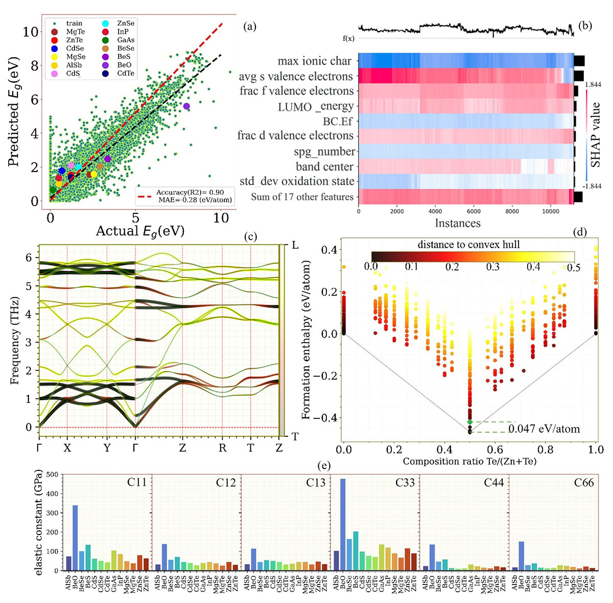
| a) The prediction results for the bandgap, and b) the heatmap of features based on the SHAP values. c) Phonon dispersions for the ZnTe compound with longitudinal and transverse phonon modes consideration, and d) convex hull diagram for the Zn–Te system. e) The elastic constants (in GPa) for all 13 final structures. (Reprinted with permission by Wiley-VCH Verlag) (click on image to enlarge) | |
| One of the key challenges in predicting new materials is assessing their stability. The researchers employed an evolutionary algorithm to search for competing crystal structures, ensuring that the predicted Haeckelite forms were indeed the most stable configuration for each elemental combination. This approach, which mimics natural selection processes, allowed the researchers to efficiently explore a vast chemical space and identify the most thermodynamically stable structures. This rigorous stability assessment led to the identification of 13 new Haeckelite compounds that are predicted to be both stable and semiconducting. | |
| Among these 13 compounds, several stand out for their potential in optoelectronic applications. For instance, aluminum antimonide (AlSb) and zinc telluride (ZnTe) in the Haeckelite structure are predicted to have indirect bandgaps in the visible light range, making them promising candidates for solar energy conversion and light-emitting devices. To put this in context, silicon, the most widely used semiconductor, has an indirect bandgap of about 1.1 eV, which limits its efficiency in certain optoelectronic applications. The predicted bandgaps of these new Haeckelite compounds fall in a range that could potentially overcome some of silicon's limitations. | |
| The researchers went beyond basic structural and electronic properties, delving into the optical characteristics of these new materials. They used the random phase approximation (RPA) method, which provides a more accurate description of electron-electron interactions than simpler models. The RPA allows researchers to calculate how electrons in a material respond collectively to external electromagnetic fields, providing insights into optical properties that are crucial for applications like solar cells and light-emitting devices. | |
| The RPA method provides a more accurate description of electron-electron interactions than simpler models, allowing researchers to calculate important optical parameters such as the dielectric function (how the material responds to electric fields), refractive index (how light bends when entering the material), and absorption coefficient (how strongly the material absorbs light at different wavelengths). | |
| Using the RPA method, the researchers calculated important optical parameters such as the dielectric function, refractive index, and absorption coefficient. These calculations revealed that some of the predicted Haeckelite compounds, particularly AlSb, InP, GaAs, and CdTe, have strong absorption in the ultraviolet and visible regions of the spectrum. This property is crucial for solar cells and photodetectors, as it determines how efficiently they can convert light into electrical energy. For comparison, gallium arsenide (GaAs), a material commonly used in high-efficiency solar cells, has strong absorption in similar spectral regions. The fact that these new Haeckelite structures show comparable properties suggests they could potentially compete with or complement existing materials in solar energy applications. | |
| Another crucial aspect for electronic applications is carrier mobility, which determines how quickly electrons can move through a material. High mobility is desirable for fast electronic devices and efficient solar cells. The researchers used sophisticated modeling techniques to predict the electron mobility in their new Haeckelite compounds. Their theoretical calculations suggest that several of the predicted materials, including GaAs, InP, CdSe, and CdTe, could potentially exhibit electron mobilities exceeding 3000 cm2 V-1 s-1 at low carrier concentrations of 1016 cm-3. | |
| To put these numbers in perspective, silicon, the backbone of modern electronics, has an electron mobility of about 1400 ccm2 V-1 s-1 under similar conditions. The potentially higher mobilities of these Haeckelite compounds could lead to faster electronic devices or more efficient solar cells. However, it's important to note that these are theoretical predictions, and actual values may differ in real materials. Nonetheless, these results highlight the potential of Haeckelite structures to outperform conventional semiconductors in certain applications. | |
| The high predicted electron mobilities are closely linked to the unique electronic structure of these Haeckelite compounds. To understand this connection, the researchers conducted a detailed analysis of the electronic band structure and density of states for each material. This analysis revealed how the arrangement of atoms in the square-octagonal Haeckelite structure influences the behavior of electrons, leading to the favorable mobility characteristics. | |
| An intriguing aspect of the predicted Haeckelite compounds is the presence of phonon gaps in some structures, such as AlSb, BeSe, BeS, InP, MgSe, and MgTe. Phonons are vibrations of atoms in a crystal lattice, similar to sound waves traveling through the material. A phonon gap is a range of vibrational energies that cannot exist in the material, analogous to how a bandgap in semiconductors represents a forbidden energy range for electrons. This feature can significantly influence a material's thermal conductivity, potentially leading to unique heat management properties. For electronic devices, where heat dissipation is often a limiting factor, materials with tunable thermal properties could be particularly valuable. | |
| The presence of phonon gaps in these Haeckelite structures is especially interesting when considered alongside their electronic properties. Materials that combine high electron mobility with controllable thermal conductivity could offer new possibilities for managing the trade-off between electrical performance and heat generation in electronic devices. | |
| While the results of this study are theoretical, they provide a solid foundation for experimental efforts to synthesize and characterize these new Haeckelite compounds. The comprehensive nature of the computational screening, encompassing structural, electronic, optical, and transport properties, offers a roadmap for experimentalists seeking to realize these materials in the laboratory. | |
| The approach demonstrated in this work exemplifies the power of combining machine learning with traditional computational methods in materials discovery. By rapidly screening a large number of potential compounds and focusing detailed calculations on the most promising candidates, the researchers were able to efficiently explore a vast chemical space and identify novel materials with desirable properties. | |
| The discovery of these new Haeckelite compounds opens up exciting possibilities for the field of optoelectronics. If successfully synthesized, these materials could lead to more efficient solar cells, faster electronic devices, and novel optical sensors. Moreover, the square-octagonal structure of Haeckelites offers unique possibilities for tuning material properties through strain engineering or chemical doping, potentially leading to a whole new class of functional materials. | |
 By
Michael
Berger
– Michael is author of three books by the Royal Society of Chemistry:
Nano-Society: Pushing the Boundaries of Technology,
Nanotechnology: The Future is Tiny, and
Nanoengineering: The Skills and Tools Making Technology Invisible
Copyright ©
Nanowerk LLC
By
Michael
Berger
– Michael is author of three books by the Royal Society of Chemistry:
Nano-Society: Pushing the Boundaries of Technology,
Nanotechnology: The Future is Tiny, and
Nanoengineering: The Skills and Tools Making Technology Invisible
Copyright ©
Nanowerk LLC
|
|
|
Become a Spotlight guest author! Join our large and growing group of guest contributors. Have you just published a scientific paper or have other exciting developments to share with the nanotechnology community? Here is how to publish on nanowerk.com. |
|