| Jun 27, 2024 | |
Papertronics devices achieve dual neuromorphic and security functions |
|
| (Nanowerk Spotlight) Paper-based electronic devices have long been an intriguing prospect for researchers, offering potential advantages in sustainability, cost-effectiveness, and flexibility. However, translating the unique properties of paper into functional electronic components has presented significant challenges. Traditional semiconductor manufacturing processes are incompatible with paper's thermal sensitivity and porous structure. Previous attempts to create paper-based electronics often resulted in devices with limited functionality or poor durability. | |
| Recent advances in materials science and nanofabrication techniques have opened new avenues for realizing sophisticated electronic devices on paper substrates. Researchers have made progress in developing conductive inks, flexible electrodes, and solution-processable semiconductors that can be applied to paper without compromising its inherent properties. These developments have paved the way for creating paper-based sensors, energy storage devices, and simple circuits. | |
| Despite these advancements, achieving complex electronic functionalities on paper, particularly in areas like neuromorphic computing and security applications, has remained elusive. Neuromorphic devices, which mimic the behavior of biological synapses, typically require precise control of charge transport and storage mechanisms. | |
| Similarly, physically unclonable functions (PUFs) used in security applications depend on the ability to generate random, unique patterns at the nanoscale level. Implementing these sophisticated functionalities on paper substrates has been a persistent challenge due to the material's inherent variability and limited compatibility with advanced fabrication techniques. | |
| A research team in Korea has now made significant strides in addressing these challenges, developing a versatile paper-based electronic device that demonstrates both neuromorphic and security capabilities. Their work, published in Advanced Materials ("Versatile Papertronics: Photo-Induced Synapse and Security Applications on Papers"), describes a novel approach to creating multifunctional "papertronics" using a combination of solution-processable materials and innovative device architectures. | |
 |
|
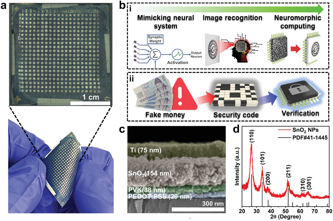
| a) Optical microscopic image. b) Schematic of the proposed devices with varying application (i: neuromorphic device, ii: security device). c) Cross-sectional SEM image of the device. d) XRD spectra of the synthesized SnO2 NPs. (Adapted from DOI:10.1002/adma.202312831 with permission by Wiley-VCH Verlag) | |
| The researchers fabricated their devices on ordinary paper substrates using a bottom-up approach. They employed a sequential deposition process involving conductive polymers, light-sensitive nanoparticles, and metal electrodes. The key components of their device were poly(9-vinylcarbazole) (PVK) and tin dioxide (SnO2) nanoparticles, which were carefully engineered to interact with ultraviolet light. | |
| One of the most notable achievements of this work is the demonstration of synaptic-like behavior in response to light stimulation. When exposed to ultraviolet pulses with a specific wavelength of 265 nm, the device exhibited characteristics reminiscent of biological synapses, including short-term and long-term plasticity. The researchers were able to modulate the device's response by varying parameters such as light intensity, pulse duration, and frequency. This light-controlled synapse-like behavior opens up possibilities for creating neuromorphic computing systems on paper substrates. | |
| The interaction between PVK and SnO2 nanoparticles under UV light is crucial to understanding the device's behavior. When 265 nm UV light is absorbed by the SnO2 nanoparticles, it generates electron-hole pairs. Some of these electrons become trapped in oxygen vacancies and other defect sites within the SnO2 nanoparticles. This trapping mechanism is responsible for the observed persistent photoconductivity and allows the device to mimic synaptic functions. The PVK layer acts as a charge transport medium and helps to modulate the overall conductivity of the device. | |
| The team showcased the potential of their device by simulating a facial recognition task. Using a simple neural network architecture and the light-responsive properties of their paper-based device, they achieved a recognition accuracy of 91.7% on a standard face database. This impressive performance was achieved with a remarkably low voltage bias of -0.01 V, demonstrating the energy efficiency of the approach. The ability to operate at such low voltages is particularly advantageous for portable and low-power applications. | |
| In addition to its neuromorphic capabilities, the device also showed promise as a physically unclonable function (PUF) for security applications. The researchers leveraged the inherent randomness in the deposition of SnO2 nanoparticles to create unique electrical characteristics in each device. By fabricating arrays of these devices on paper, they generated security keys that exhibited high levels of randomness and uniqueness. | |
| The team evaluated the performance of their PUF devices using standard metrics such as uniformity and inter-Hamming distance. Their results showed values close to the ideal 50% for both metrics, indicating excellent randomness and distinguishability between different devices. Importantly, the security keys generated by these paper-based PUFs remained stable even after 210 days of storage and when subjected to bending stresses with a curvature radius of 8.75 mm, demonstrating their potential for real-world applications in anti-counterfeiting and secure authentication. | |
| The researchers conducted extensive stability tests to ensure the robustness of their devices. They exposed the devices to various stress conditions, including prolonged air exposure, voltage stress, and continuous UV irradiation. Remarkably, the devices maintained their electrical properties and functional characteristics even after 210 days of air exposure. Voltage stress tests, involving the application of -0.1 V and -0.5 V for 1000 seconds each, showed only minimal changes in current levels. Similarly, continuous UV exposure (265 nm, 2.3 mW cm-2) for 900 seconds did not significantly alter the device performance. These results highlight the exceptional stability of the paper-based devices, addressing a common concern in flexible electronics. | |
| One of the most intriguing aspects of this research is the dual functionality achieved with a single device structure. The ability to serve as both a neuromorphic component and a security element could lead to the development of highly integrated, secure edge computing devices on paper substrates. This convergence of functionalities addresses growing concerns about data privacy and security in Internet of Things (IoT) applications. | |
| The researchers' approach also offers several practical advantages. The use of solution-processable materials and room-temperature fabrication techniques makes their devices compatible with large-scale, low-cost manufacturing processes. The flexibility and eco-friendliness of paper substrates further enhance the potential for widespread adoption of this technology. | |
| While this work represents a significant advance in paper-based electronics, several challenges remain to be addressed before practical applications can be realized. Improving the long-term stability of these devices in various environmental conditions, increasing their operational speed, and scaling up manufacturing processes are areas that require further investigation. | |
| Looking ahead, the researchers suggest potential avenues for future development. One promising direction is the integration of active devices, such as transistors, to create fully self-operating papertronic systems. They also propose exploring techniques like laser-induced graphene (LIG) electrode printing directly onto paper substrates, which could further enhance the sustainability and manufacturability of paper-based electronics. Additionally, the team envisions incorporating other flexible materials and polymers to expand the range of possible applications and improve device performance. | |
 By
Michael
Berger
– Michael is author of three books by the Royal Society of Chemistry:
Nano-Society: Pushing the Boundaries of Technology,
Nanotechnology: The Future is Tiny, and
Nanoengineering: The Skills and Tools Making Technology Invisible
Copyright ©
Nanowerk LLC
By
Michael
Berger
– Michael is author of three books by the Royal Society of Chemistry:
Nano-Society: Pushing the Boundaries of Technology,
Nanotechnology: The Future is Tiny, and
Nanoengineering: The Skills and Tools Making Technology Invisible
Copyright ©
Nanowerk LLC
|
|
|
Become a Spotlight guest author! Join our large and growing group of guest contributors. Have you just published a scientific paper or have other exciting developments to share with the nanotechnology community? Here is how to publish on nanowerk.com. |
|