| Jun 26, 2024 | |
Graphene boosts UV-C LED efficiency for sterilization |
|
| (Nanowerk Spotlight) Ultraviolet light has long been recognized as a powerful tool for disinfection and sterilization. Its ability to neutralize harmful microorganisms has made it invaluable in applications ranging from water purification to medical equipment sterilization. Traditionally, this ultraviolet light has been produced by mercury vapor lamps, which are effective but come with significant drawbacks. These lamps are bulky, fragile, and contain toxic mercury, making them less than ideal for many modern applications. | |
| The advent of light-emitting diodes (LEDs) revolutionized lighting technology in the visible spectrum, offering compact, energy-efficient, and long-lasting alternatives to traditional light sources. Naturally, researchers and engineers sought to extend these benefits to the ultraviolet range, particularly the UV-C spectrum (wavelengths between 100-280 nanometers) most effective for disinfection. However, the development of UV-C LEDs has faced numerous technical challenges that have limited their widespread adoption. | |
| The primary obstacle in creating efficient UV-C LEDs lies in the fundamental properties of the materials required to produce such short-wavelength light. Unlike visible LEDs, which can use relatively simple semiconductor materials, UV-C LEDs require complex alloys of aluminum, gallium, and nitrogen (AlGaN). These materials are difficult to grow with the necessary crystal quality and present significant challenges in terms of electrical conductivity and light extraction. | |
| One persistent issue has been the poor electrical conductivity of p-type AlGaN, the layer responsible for injecting positive charge carriers (holes) into the LED's active region. This low conductivity leads to high operating voltages and inefficient current spreading across the device. Another challenge has been the lack of transparent conductive materials suitable for use in the UV-C range. Traditional transparent conductors used in visible LEDs, such as indium tin oxide, become opaque at these short wavelengths. | |
| Over the years, researchers have explored various approaches to overcome these limitations. Efforts have focused on improving the crystal quality of AlGaN layers, developing novel doping techniques, and engineering device structures to enhance light extraction. One promising avenue has been the use of flip-chip designs, where the LED is mounted upside down and light is emitted through the transparent substrate. However, these designs often require expensive materials like rhodium for mirror contacts, limiting their commercial viability. | |
| The search for suitable transparent conductive materials for UV-C LEDs has led researchers to explore two-dimensional materials, with graphene emerging as a particularly promising candidate. Graphene's unique combination of high electrical conductivity and optical transparency makes it potentially ideal for use in UV-C LEDs. However, previous attempts to incorporate graphene into these devices have primarily relied on transfer methods, which introduce defects and impurities that compromise performance. | |
| A recent study published in Advanced Materials ("Graphene-Enhanced UV-C LEDs") by researchers from the University of Duisburg-Essen presents a novel approach to integrating graphene into UV-C LEDs, potentially addressing several long-standing challenges in the field. The team developed a method to grow high-quality graphene directly on the p-AlGaN layer of UV-C LED wafers using a technique called plasma-enhanced chemical vapor deposition (PECVD). | |
 |
|
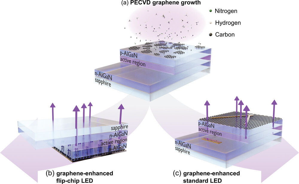
| Scheme of graphene-enhanced UV-C LEDs. a) PECVD growth process of the graphene on the UV-C LED. b) UV-C LED in flip-chip design with an Al mirror and a graphene interlayer on the p-AlGaN layer. c) UV-C LED in standard geometry with graphene as a current spreading layer. (Image: Reproduced from DOI:10.1002/adma.202313037 CC BY) | |
| This direct growth technique eliminates the need for graphene transfer, resulting in a cleaner interface and better electrical contact between the graphene and the semiconductor layers. The researchers optimized the growth conditions to produce graphene with over 90% transparency in the UV-C range and a sheet resistance below 3,000 ohms per square, striking a balance between optical and electrical properties crucial for LED performance. | |
| The team explored two distinct device architectures leveraging their graphene integration technique. In a flip-chip configuration, they used graphene as an interlayer between the p-AlGaN and an aluminum mirror contact. This approach yielded devices with external quantum efficiencies (EQE) of up to 9.5% at an operating voltage of 8 volts. The EQE is a measure of how efficiently the LED converts electrical energy into usable light output. By incorporating a thin layer of nickel oxide along with the graphene, they further reduced the turn-on voltage to 4.5 volts, addressing a common issue in UV-C LEDs that often require high operating voltages. | |
| Perhaps even more significantly, the researchers demonstrated the potential of graphene as a transparent current spreading layer in a standard (top-emitting) LED geometry. This configuration has traditionally been challenging for UV-C LEDs due to the lack of suitable transparent conductive materials. The graphene layer enabled uniform current spreading over an area of approximately 1 square millimeter, resulting in devices with EQEs exceeding 2% when measured from the top surface. While this efficiency is lower than that achieved in the flip-chip design, it represents a significant advancement for top-emitting UV-C LEDs, which have struggled to reach 1% EQE in previous studies. | |
| The success of this approach lies in the careful optimization of the graphene growth process. The researchers fine-tuned parameters such as growth temperature, time, and gas composition to produce graphene with the desired properties directly on the LED wafer. They used Raman spectroscopy, a technique that analyzes the vibrations of atoms in a material, to confirm the high quality and uniformity of the graphene layers. Optical transmission measurements further verified the graphene's transparency in the UV-C range. | |
| This work demonstrates the versatility of graphene in addressing multiple challenges in UV-C LED design. As an interlayer in flip-chip devices, it enables the use of cost-effective aluminum mirrors while maintaining low turn-on voltages and high efficiencies. In top-emitting devices, it serves as a transparent current spreading layer, opening up new possibilities for UV-C LED architectures and applications. | |
| The implications of this research extend beyond the immediate improvements in device performance. The ability to grow high-quality graphene directly on AlGaN surfaces could enable new device concepts and integration strategies in the broader field of UV optoelectronics. Moreover, the demonstrated compatibility of the graphene growth process with existing LED fabrication techniques suggests a potential path for scalable manufacturing of graphene-enhanced UV-C LEDs. | |
| While the efficiencies achieved in this study are still below those of state-of-the-art visible LEDs, they represent a significant step forward for UV-C devices. The combination of improved efficiency, lower operating voltages, and potentially simpler fabrication processes could accelerate the adoption of UV-C LEDs in applications such as water and air purification, surface disinfection, and medical treatments. | |
| This research opens new avenues for the development of UV-C LEDs, demonstrating the potential of graphene to address long-standing challenges in the field. However, as with any emerging technology, challenges remain. The long-term stability of graphene-enhanced UV-C LEDs under high-power operation and harsh environmental conditions needs to be thoroughly investigated. Additionally, further optimization of the device structure and graphene growth process could yield additional performance improvements. | |
 By
Michael
Berger
– Michael is author of three books by the Royal Society of Chemistry:
Nano-Society: Pushing the Boundaries of Technology,
Nanotechnology: The Future is Tiny, and
Nanoengineering: The Skills and Tools Making Technology Invisible
Copyright ©
Nanowerk LLC
By
Michael
Berger
– Michael is author of three books by the Royal Society of Chemistry:
Nano-Society: Pushing the Boundaries of Technology,
Nanotechnology: The Future is Tiny, and
Nanoengineering: The Skills and Tools Making Technology Invisible
Copyright ©
Nanowerk LLC
|
|
|
Become a Spotlight guest author! Join our large and growing group of guest contributors. Have you just published a scientific paper or have other exciting developments to share with the nanotechnology community? Here is how to publish on nanowerk.com. |
|