| May 21, 2024 | |
Printed organic transistors achieve record performance and 3D circuit density |
|
| (Nanowerk Spotlight) Organic semiconductors have long held promise for enabling deformable electronic devices that can be manufactured at low cost and high volumes using printing techniques. However, realizing this vision has been hampered by the relatively poor performance and non-uniformity of printed organic transistors compared to those made with conventional silicon. Organic semiconductor films tend to have significant morphological and energetic disorder that limits charge transport. | |
| To address this, much research has focused on increasing the crystallinity of polymer films to improve mobility. But an alternative approach emerged with the development of IDT-BT (indacenodithiophene-co-benzothiadiazole), a donor-acceptor copolymer that exhibits high mobility in an amorphous, disordered state due to its planar, rigid backbone. This allows high performance without the need for strict processing conditions to induce crystallinity. | |
| It's against this backdrop that a team of scientists has developed a new set of materials and fabrication methods for printed organic electronics. They reported their findings in Advanced Functional Materials ("High Mobility Amorphous Polymer-Based 3D Stacked Pseudo Logic Circuits through Precision Printing"). | |
 |
|
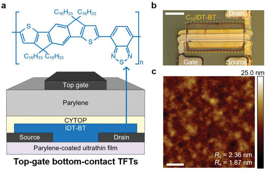
| a) Molecular structure of IDT-BT and schematic cross-section of a printed transistor with top-gate bottom-contact configuration. b) Microscopic image of the fabricated device (scale bar, 500 µm). The dimensions of the device are L = 40 µm and W = 1500 µm. c) AFM topology image of the printed transistors (scan size, 2 × 2 µm; scale bar, 400 nm). (Reprinted from DOI:10.1002/adfm.202312922, CC BY) | |
| By optimizing printing techniques for IDT-BT, they've achieved record-setting performance and uniformity for printed transistor arrays. And by leveraging the unique properties of IDT-BT, they've realized complex integrated circuits in a fully printed, flexible form factor. | |
| The resulting devices showed hole mobilities exceeding 1 cm2/Vs, current on/off ratios greater than 107, and subthreshold slopes of 251 mV/dec (meaning that a change of 251 millivolts in the gate voltage results in a tenfold increase in the current) – characteristics on par with or exceeding the best printed organic transistors to date. | |
| Remarkably, arrays of 256 transistors fabricated in this manner had 100% yield, with excellent device-to-device uniformity. Statistical analysis revealed very tight distributions in mobility and threshold voltage, with 9.55% and 4.51% relative standard deviation respectively. | |
| The amorphous nature of IDT-BT also proved advantageous for realizing 3D-stacked devices. By leveraging the low thermal budget required for processing this material, the team fabricated stacks of five transistors on top of each other without any degradation in the bottom devices. This 3D monolithic integration is crucial for increasing transistor density. | |
| To demonstrate the potential of this technology, the researchers devised a novel 3D NAND logic gate. Using just four vertically stacked transistors, they implemented the functionality of a six-transistor 2D NAND with a footprint six times smaller. Arrays of these 3D NAND gates showed outstanding consistency, with voltage gains up to 33.9 V/V - significantly higher than other printed organic circuits. | |
| Interconnecting multiple 3D NAND gates, the team built other logic gates like NOT, buffer, and AND. Notably, they achieved a record-high density of 100 printed transistors per square centimeter. At this density level, approximately 4500 transistors could fit on the area of an adult hand - comparable to the transistor count of 8-bit microprocessors from the early days of computing. | |
 |
|
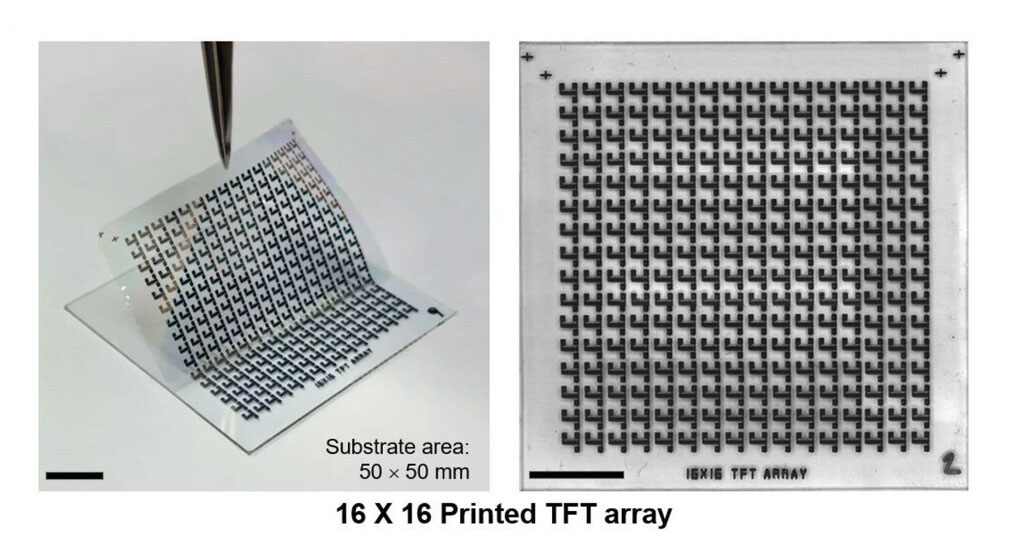
| Photographs of flexible printed 16 x 16 thin-film transistor array. (scale bar, 10 mm).(Reprinted from DOI:10.1002/adfm.202312922, CC BY) | |
| This work marks a major step forward in printed organic electronics, addressing many of the challenges that have limited their practicality. The combination of high-performance IDT-BT semiconductor, optimized printing processes, and 3D integration puts low-cost, flexible circuits within reach for applications like display backplanes, sensors, and wearable devices. With further scaling, this technology could even enable a new era of printable computing. | |
| Still, challenges remain in improving the stability and reproducibility of these devices for commercial manufacturing. And increasing mobility even further will be important for applications like OLED displays that require higher drive currents. But the advancements made here provide a promising foundation for continued innovation in this field, which could reshape entire industries with the advent of ubiquitous flexible electronics. | |
 By
Michael
Berger
– Michael is author of three books by the Royal Society of Chemistry:
Nano-Society: Pushing the Boundaries of Technology,
Nanotechnology: The Future is Tiny, and
Nanoengineering: The Skills and Tools Making Technology Invisible
Copyright ©
Nanowerk LLC
By
Michael
Berger
– Michael is author of three books by the Royal Society of Chemistry:
Nano-Society: Pushing the Boundaries of Technology,
Nanotechnology: The Future is Tiny, and
Nanoengineering: The Skills and Tools Making Technology Invisible
Copyright ©
Nanowerk LLC
|
|
|
Become a Spotlight guest author! Join our large and growing group of guest contributors. Have you just published a scientific paper or have other exciting developments to share with the nanotechnology community? Here is how to publish on nanowerk.com. |
|