| Sep 17, 2024 |
New mechanism explains rapid energy sharing across atomic semiconductor junctions
(Nanowerk News) Researchers have discovered a new mechanism for energy sharing in tiny interfaces in semiconductors, the components at the heart of our electronic devices. This mechanism arises from the close coupling between electrons and atomic vibrations. Researchers made a sandwich of atomically thin layers and used short pulses of light to push electrons across the interface. They then used an ultrafast beam of electrons to capture the atomic motions triggered by this electron transfer.
|
|
Even though only one atomic layer was photoexcited, both layers heated up at nearly the same time. The research found that this ultrafast transfer of heat occurs thanks to electrons using an interlayer "bridge" state to flow across the interface, triggering atomic vibrations (heat) in their wake.
|
|
Understanding and controlling heat flow is critical for many applications, especially for electronic devices. As these devices become increasingly miniaturized, the interfaces between materials often become the bottleneck to removing heat.
|
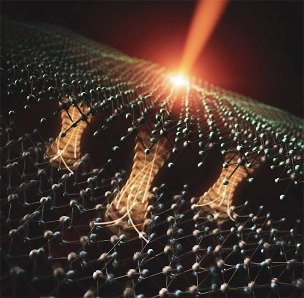 |
| Illustration of electron transfer driven by an ultrashort laser pulse across an interface between two atomically thin materials. An electronic interlayer “bridge” state emitting lattice vibrations in the layers facilitates this electron transfer. (Image: SLAC National Accelerator Laboratory)
|
|
In this research (Nature Nanotechnology, "Bidirectional phonon emission in two-dimensional heterostructures triggered by ultrafast charge transfer"), scientists uncovered a new mechanism for the transfer of energy across an interface.
|
|
Electrons play a key role in this transfer, and the flow of electrons can, in principle, be controlled using external fields. This means that the mechanism could enable precise control over the generation of heat at the atomic scale. This work improves our fundamental understanding of energy dissipation. This knowledge is crucial for making nanoscale electronic devices that are more energy efficient.
|
|
Heat generation in electronic and optical devices during operation is a critical aspect of their performance, especially as devices become smaller. Here, researchers directly probed the flow of heat across a junction of two atomically thin semiconductors on ultrafast timescales. They found that when short pulses of light were used to inject charge carriers into one of the layers, both layers heated up nearly simultaneously. This could not be explained simply by the transfer of heat via atomic vibrations.
|
|
Instead, the team’s theoretical calculations showed that this observation was consistent with a mechanism involving interlayer transfer of electrons through a hybridized state or “bridge” state across the heterostructure of WSe2/WS2 monolayers. The results provide a new fundamental understanding of how charge carriers impact heat generation in nanoscale devices.
|
|
This highly collaborative work was enabled by three Department of Energy (DOE) Office of Science user facilities. The nanoscale semiconductor junctions in this work were fabricated at the Molecular Foundry at Lawrence Berkeley National Laboratory. The ultrafast electron diffraction work was conducted at the MeV ultrafast electron diffraction beamline of the Linac Coherent Light Source at SLAC National Accelerator Laboratory. The computational work used resources at the National Energy Research Scientific Computing Center at Lawrence Berkeley National Laboratory and at the Texas Advanced Computing Center.
|
