| Jul 08, 2024 |
Flexible nanoimprint lithography enables efficient fabrication of biomimetic microstructures
(Nanowerk News) Gallium nitride (GaN)-based light-emitting diodes (LEDs) have transformed the lighting industry by replacing conventional lighting technologies with superior energy efficiency, longer operating life and greater environmental sustainability.
|
|
In recent years, considerable attention has been paid to the trend toward miniaturization of LEDs, driven by display devices, augmented reality, virtual reality, and other emerging technologies. Due to the lack of cost-effective native substrates, the presence of high threading dislocation density in heteroepitaxial films grown on sapphire substrate is a major limiting factor for device performance.
|
|
In addition, Fresnel reflections at the interface between epitaxy and substrate caused by abrupt changes in the refractive indices of the material reduce the light energy utilization.
|
|
Distributed nano-nipple array on the compound eyes of moth-like animals have excellent anti-reflective ability and strong light-absorption capacity, which provides great inspiration for improving light utilization. However, rapid and precise processing of microstructures on curved surfaces of optoelectronic devices is highly challenging.
|
|
“The common projection lithography methods are very sensitive to the shape of the substrate, so the accuracy of microstructure definition may be reduced when the substrate has large warps or irregular shapes. We propose a flexible nanoimprint lithography technique that enables high-throughput and high-quality processing of bionic microstructures on curved surfaces,” says Professor Shengjun Zhou.
|
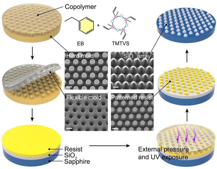 |
| Fabrication of microstructures through steps of thermo-compression molding, imprinting, UV exposure and two-step etching process. (Image: Science China Press)
|
|
The researchers first carried out the design of bionic microstructure array and flexible nanoimprinting molds. The fabrication of the microstructures was realized by thermo-compression molding, imprinting, UV exposure and a specially designed two-step etching process to obtain a compound-eye-like silica microstructures (NCSM) template. It is shown that flexible nanoimprinting has adaptability to substrate warpage, allows precise definition of microstructures, and provides good durability. Compared to projection lithography, productivity was increased by a factor of 6.4 and economic cost savings of 25% were achieved.
|
|
The researchers investigated the growth behavior of GaN crystals on NCSM template by epitaxial growth interruption experiments. They found that adjusting the morphology of the nucleation layer by the NCSM template helps to control the growth orientation of GaN and obtain epitaxial films with low dislocation density. In addition, the NCSM template can significantly improve the light extraction efficiency of the devices owing to the modulation of photons by the bionic microstructures.
|
|
Professor Sheng Liu says, “Thanks to these two improvements, the light output capability of mini-LEDs based on NCSM template has been greatly enhanced.” He concludes, “This study is promising for the efficient fabrication of microstructures and performance enhancement of optoelectronic devices. In the future, we will continue to explore flexible nanoimprinting technique and expect it to show broader applications.”
|
|
This work has been published in Science Bulletin ("Flexible nanoimprint lithography enables high-throughput manufacturing of bioinspired microstructures on warped substrates for efficient III-nitride optoelectronic devices").
|
