| Jun 07, 2024 |
New light-activated electron pathway found in nanotubes
(Nanowerk News) Research groups led by the University of Tsukuba and the University of Rennes have unveiled a unique phenomenon where, upon exposure to light, a nested structure of carbon nanotubes enveloped in boron nitride nanotubes allows for a peculiar electron escape route. This discovery opens up exciting possibilities for various applications, including creating high-speed optical devices, fast control of electrons and other particles generated by exposure to light, and effective heat dissipation from devices.
|
|
Recent studies have shown that materials composed of layered of tubes (known as low-dimensional materials) that are atomic-thick, can exhibit new properties. The static properties of these structures, such as electrical conduction, have been widely studied. However, their dynamic properties, such as the electronic transfer between layers and the atomic motion triggered by light exposure, have been explored to a lesser degree.
|
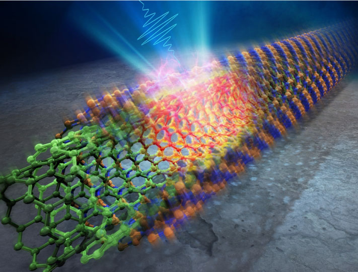 |
| Photoinduced dynamics during electronic transfer from narrow to wide bandgap layers in one-dimensional heterostructured materials. (Image: University of Rennes)
|
|
In this study (Nature Communications, "Photoinduced dynamics during electronic transfer from narrow to wide bandgap layers in one-dimensional heterostructured materials"), researchers created nested cylindrical structures by wrapping carbon nanotubes (CNTs) in boron nitride nanotubes (BNNTs). They then observed the motion of electrons and atoms induced by ultrashort light exposure on a 1D material.
|
|
The electron motion was monitored using broadband ultrafast optical spectroscopy measurements, which can capture the instantaneous changes in molecular and electronic structures caused by light irradiation with an accuracy of ten trillionths of a second (10-13s). The motion of atoms was observed using ultrafast time-resolved electron diffraction, which can monitor structural dynamics with an accuracy of a trillionth of a second (10-12s).
|
|
The researchers discovered that when different types of low-dimensional materials are stacked together, a pathway (or channel) is created that allows electrons to escape from a given sub-part in the material. They also discovered that electrons generated by exposing CNTs to light can be transferred into BNNTs through these electronic channels. The energy of these excited electrons is rapidly converted into thermal energy within the BNNTs, facilitating an extremely fast conversion into thermal energy.
|
|
This research has revealed a new physical phenomenon that occurs at the interface between two different materials. In addition to the ultrafast transport of thermal energy, this phenomenon could potentially be applied to a range of new technologies, including the development of ultrafast optical devices and the ultrafast manipulation of electrons and holes generated by exposure to light.
|
