| May 28, 2024 |
Better cameras with perovskite
(Nanowerk News) Family, friends, vacations, pets: Today, we take photos of everything that comes in front of our lens. Digital photography, whether with a cell phone or camera, is simple and hence widespread. Every year, the latest devices promise an even better image sensor with even more megapixels.
|
|
The most common type of sensor is based on silicon, which is divided into individual pixels for red, green and blue (RGB) light using special filters. However, this is not the only way to make a digital image sensor – and possibly not even the best.
|
|
A consortium comprising Maksym Kovalenko from Empa's Thin Films and Photovoltaics laboratory, Ivan Shorubalko from Empa's Transport at Nanoscale Interfaces laboratory, as well as ETH Zurich researchers Taekwang Jang and Sergii Yakunin, is working on an image sensor made of perovskite capable of capturing considerably more light than its silicon counterpart. In a silicon image sensor, the RGB pixels are arranged next to each other in a grid. Each pixel only captures around one-third of the light that reaches it. The remaining two-thirds are blocked by the color filter.
|
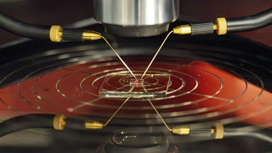 |
| Innovative light sensor: The researchers are now working on miniaturizing the pixels, which were originally up to five millimeters in size, and assembling them into a functioning image sensor. (Image: Empa)
|
|
Pixels made of lead halide perovskites do not need an additional filter: it is already "built into" the material, so to speak. Empa and ETH researchers have succeeded in producing lead halide perovskites in such a way that they only absorb the light of a certain wavelength – and therefore color – but are transparent to the other wavelengths. This means that the pixels for red, green and blue can be stacked on top of each other instead of being arranged next to each other.
|
|
The resulting pixel can absorb the entire wavelength spectrum of visible light. "A perovskite sensor could therefore capture three times as much light per area as a conventional silicon sensor," explains Empa researcher Shorubalko. Moreover, perovskite converts a larger proportion of the absorbed light into an electrical signal, which makes the image sensor even more efficient.
|
|
Kovalenko's team was first able to fabricate individual functioning stacked perovskite pixels in 2017. To make the next step towards real image sensors, the ETH-Empa consortium led by Kovalenko had partnered with the electronics industry.
|
|
"The challenges to address include finding new materials fabrication and patterning processes, as well as design and implementation of the perovskite-compatible read-out electronic architectures", emphasizes Kovalenko. The researchers are now working on miniaturizing the pixels, which were originally up to five millimeters in size, and assembling them into a functioning image sensor.
|
|
"In the laboratory, we don't produce the large sensors with several megapixels that are used in cameras," explains Shorubalko, "but with a sensor size of around 100'000 pixels, we can already show that the technology works.
|
|
|
|
The advantages of perovskite-based image sensors (top) are apparent. Illustration: Empa
|
Good performance with less energy
|
|
Another advantage of perovskite-based image sensors is their manufacture. Unlike other semiconductors, perovskites are less sensitive to material defects and can therefore be fabricated relatively easily, for example by depositing them from a solution onto the carrier material. Conventional image sensors, on the other hand, require high-purity monocrystalline silicon, which is produced in a slow process at almost 1500 degrees Celsius.
|
|
The advantages of perovskite-based image sensors are apparent. It is therefore not surprising that the research project also includes a partnership with industry. The challenge lies in the stability of perovskite, which is more sensitive to environmental influences than silicon.
|
|
"Standard processes would destroy the material," says Shorubalko. "So we are developing new processes in which the perovskite remains stable. And our partner groups at ETH Zurich are working on ensuring the stability of the image sensor during operation."
|
|
If the project, which will run until the end of 2025, is successful, the technology will be ready for transfer to industry. Shorubalko is confident that the promise of a better image sensor will attract cell phone manufacturers.
|
|
"Many people today choose their smartphone based on the camera quality because they no longer have a stand-alone camera," says the researcher. A sensor delivering excellent images in much poorer lighting conditions could be a major advantage.
|
