The new 2D frontier of Silicene, Stanene, Germanene, Antimonene, and Phosphorene
Imagine a material so thin that it consists of a single layer of atoms, yet it possesses strength, flexibility, and electrical properties that outmatch those of materials thousands of times thicker. This is the essence of two-dimensional (2D) materials, a class of materials that are only one atom thick, making them essentially two-dimensional. They have gained immense interest for their potential to revolutionize industries ranging from electronics and energy to medicine and beyond. The unique aspect of 2D materials lies in their surface; since all atoms are exposed, their electronic, optical, and chemical properties are remarkably different from their bulk counterparts.
2D materials are important because they offer a new toolkit for solving technological challenges, such as making electronics faster and more energy-efficient or creating sensors that are incredibly sensitive. Their thinness and high surface area make them ideal for applications where space and efficiency are critical.
What Makes This Specific Group of 2D Materials Unique
Silicene, stanene, germanene, antimonene, and phosphorene, composed of single elements from groups 14 and 15 of the periodic table, represent a fascinating subset of 2D materials that are not as widely recognized as graphene but offer their own unique advantages. Their discovery has not only expanded the family of 2D materials but also introduced new possibilities for band gap engineering, a critical aspect in the development of next-generation electronic and optoelectronic devices.
Unlike graphene, which is a zero-gap semiconductor, these materials possess tuneable electronic properties, including variable band gaps. This means they can be engineered to either conduct electricity with no resistance or act as insulators, depending on their structure and the application needs. This versatility is crucial for the development of next-generation electronic devices, photovoltaics, and nanoscale transistors.
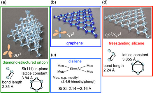
Silicene
Silicene is a two-dimensional allotrope of silicon, sharing a similar honeycomb lattice structure with graphene. However, due to the larger size of silicon atoms, silicene exhibits a slightly buckled structure. This characteristic buckling grants significant advantages: it allows for easier manipulation of silicene's electronic properties through external electric fields, leading to potential applications in highly efficient transistors. Moreover, silicene possesses a tunable band gap that can range from semimetallic to semiconducting, making it versatile for various electronic components.
Silicene exhibits high electrical conductivity and displays the quantum Hall effect at low temperatures. Importantly, silicene's compatibility with existing silicon-based electronics makes it a highly promising material for next-generation nanoelectronics and quantum computing. However, its instability in air remains a challenge that needs to be addressed for widespread practical applications.
Read more:
Stanene
Stanene is a two-dimensional material composed of tin atoms arranged in a honeycomb lattice. It is predicted to be a topological insulator, meaning it can conduct electricity without resistance along its edges while remaining insulating in its interior. This unique property holds significant potential for revolutionizing energy-efficient electronics, including applications in spintronics and quantum computing.
Of particular interest is stanene's potential to conduct electricity without loss at room temperature when functionalized with fluorine. This could transform the field of electrical conductivity. Additionally, stanene's structure allows for a versatile combination of flexibility and robustness when conducting electrical currents.
Read more:
Germanene
Germanene is a two-dimensional allotrope of germanium, featuring a honeycomb lattice structure similar to graphene, silicene, and stanene. Like silicene, it exhibits a puckered structure due to the size of germanium atoms. This attribute grants it both flexibility and unique electronic properties, including a tunable band gap that can be adjusted through chemical modifications. This makes germanene suitable for optoelectronic applications such as flexible displays and advanced photovoltaic cells.
Germanene is predicted to be a topological insulator, holding further promise for electronics. Moreover, germanene's successful synthesis on metallic substrates underscores its potential for integration into future technological advancements.
Read more:
Antimonene
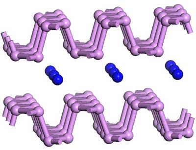
Antimonene is a two-dimensional material composed of a single layer of antimony atoms arranged in a puckered structure. It is notable for its stability under ambient conditions and its tunable semiconducting properties. The band gap of antimonene can be adjusted by varying the number of layers and through external stimuli. This variability makes antimonene highly versatile for applications in semiconductors, batteries, photocatalysis, and electronic and optical devices. Additionally, antimonene's biocompatibility opens up exciting possibilities for its use in biomedical applications.
Read more:
Phosphorene
Phosphorene, a single layer of phosphorus atoms, possesses a distinctive puckered structure that sets it apart from the flat lattices of graphene and its analogs. This structure results in anisotropic electrical, thermal, and mechanical properties, offering exceptional versatility for electronic and optoelectronic applications.
Phosphorene boasts a direct bandgap, enabling efficient light absorption and emission, which holds great promise for advancements in photodetectors, solar cells, and LEDs. Additionally, its high carrier mobility and wide-ranging bandgap make it exceptionally attractive for transistors, sensors, and photovoltaic devices. The anisotropic nature of phosphorene, stemming from its structure, could lead to the development of innovative electronic and optoelectronic devices with unique functionalities.
Read more:
Practical Limitations and Challenges
Currently, synthesizing these materials with high quality and on a large scale is akin to trying to paint a masterpiece on a grain of rice. Their sensitivity to air and moisture makes them challenging to work with outside of controlled laboratory environments. Overcoming these challenges could lead to a revolution in how we make and use electronic devices, making them more integrated into our daily lives and significantly more energy-efficient.
Resolving these synthesis and stability challenges is crucial. Achieving this would not only unlock the full potential of these materials but also pave the way for their integration into everyday technology, marking a significant leap forward in the development of advanced technologies and sustainable solutions.
However, this dynamic field of 2D materials research is continuously evolving, with scientists making significant strides in overcoming the synthesis and stability challenges associated with these materials. Recent breakthroughs include:
- Silicene: Successful synthesis on insulating substrates, preserving its electronic properties while offering a pathway towards integrating silicene into practical electronic devices.
- Stanene: Theoretical predictions suggest stanene could conduct electricity with 100% efficiency at room temperature. Efforts are now focused on stabilizing stanene in a way that retains its predicted properties in real-world applications.
- Germanene: Progress in layering germanene on substrates that do not disrupt its electronic properties, moving closer to its use in electronics.
- Antimonene: Advances in exfoliation techniques have allowed for the production of antimonene flakes with enhanced stability and suitability for a variety of applications.
- Phosphorene: Innovations in encapsulation methods have significantly improved phosphorene's air stability, making it more practical for use in electronic devices.
These advancements highlight the field's momentum towards making these futuristic materials a part of our everyday technology, addressing the synthesis and stability challenges head-on. As research progresses, we edge closer to unlocking the full potential of these materials, heralding a new era of technological innovation.