Nanoribbons: Unlocking Novel Properties Through One-Dimensional Nanostructures
What are Nanoribbons?
Nanoribbons are one-dimensional nanostructures with a thickness and width in the nanoscale range, typically below 100 nanometers. These ribbon-like structures are characterized by their high aspect ratio, with lengths that can extend to micrometers or even millimeters. Nanoribbons can be composed of various materials, including semiconductors, metals, and graphene, each exhibiting unique electronic, optical, and mechanical properties.
Types of Nanoribbons
Nanoribbons can be classified based on their composition and edge structure:
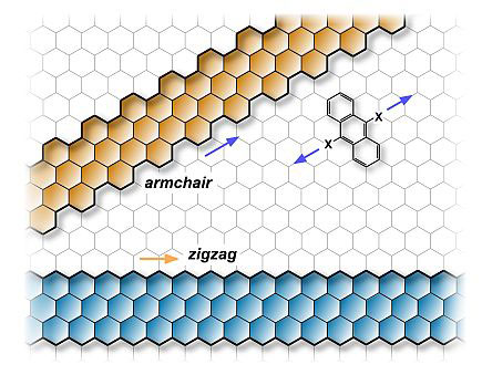
Graphene Nanoribbons (GNRs)
Graphene nanoribbons are narrow strips of graphene, a single layer of carbon atoms arranged in a hexagonal lattice. GNRs can have different edge structures, such as armchair or zigzag, which significantly influence their electronic properties. Armchair GNRs can be either metallic or semiconducting, depending on their width, while zigzag GNRs exhibit localized edge states and magnetic properties.
Semiconductor Nanoribbons
Semiconductor nanoribbons, such as silicon, germanium, and III-V compounds (e.g., GaAs, InP), are promising building blocks for nanoelectronic devices. These nanoribbons can be synthesized through top-down approaches, such as lithography and etching, or bottom-up methods, like vapor-liquid-solid (VLS) growth. Semiconductor nanoribbons exhibit quantum confinement effects and can be used in transistors, sensors, and photovoltaic devices.
Metal Nanoribbons
Metal nanoribbons, such as gold, silver, and copper, are of interest for their plasmonic properties and applications in nanophotonics. These nanoribbons can support surface plasmon polaritons (SPPs), which are electromagnetic waves coupled to the collective oscillations of free electrons at the metal surface. Metal nanoribbons can be used in plasmonic waveguides, nanoantennas, and surface-enhanced Raman spectroscopy (SERS) substrates.
Synthesis Methods
Several synthesis methods have been developed to fabricate nanoribbons with controlled dimensions and properties:
Top-Down Approaches
Top-down approaches involve the patterning and etching of thin films to create nanoribbon structures. Lithographic techniques, such as electron beam lithography (EBL) and nanoimprint lithography (NIL), are commonly used to define the nanoribbon patterns. Subsequent etching processes, like reactive ion etching (RIE) or wet chemical etching, are employed to transfer the patterns onto the desired material.
Bottom-Up Approaches
Bottom-up approaches rely on the self-assembly or controlled growth of nanoribbons from molecular precursors or nanoparticles. VLS growth is a widely used method for synthesizing semiconductor nanoribbons, where a metal catalyst (e.g., gold) directs the one-dimensional growth of the nanoribbon. Other bottom-up methods include chemical vapor deposition (CVD), solution-phase synthesis, and template-assisted growth.
Properties and Applications
Nanoribbons exhibit unique properties that arise from their one-dimensional geometry and quantum confinement effects:
Electronic Properties
Nanoribbons can display metallic, semiconducting, or insulating behavior, depending on their composition, width, and edge structure. The electronic band structure of nanoribbons is strongly influenced by quantum confinement, leading to the opening of a bandgap in semiconducting nanoribbons. This allows for the tuning of electronic properties by controlling the nanoribbon dimensions, enabling their use in nanoelectronic devices such as field-effect transistors, sensors, and interconnects.
Optical Properties
Nanoribbons can exhibit distinctive optical properties, such as strong light absorption, emission, and nonlinear optical effects. Semiconductor nanoribbons can have size-dependent bandgaps, leading to tunable optical properties in the visible and near-infrared range. Metal nanoribbons can support localized surface plasmon resonances (LSPRs), enabling enhanced light-matter interactions and applications in nanophotonics, such as plasmonic waveguides, nanolasers, and optical sensors.
Mechanical Properties
Nanoribbons can possess exceptional mechanical properties, such as high strength, flexibility, and toughness. Graphene nanoribbons, in particular, have shown remarkable mechanical performance, with a Young's modulus exceeding 1 TPa and a tensile strength approaching 100 GPa. The mechanical robustness of nanoribbons makes them promising candidates for flexible electronics, nanoelectromechanical systems (NEMS), and reinforcement materials in nanocomposites.
Challenges and Future Perspectives
Despite the significant progress in nanoribbon research, several challenges need to be addressed for their large-scale integration and practical applications. One of the main challenges is the precise control over nanoribbon dimensions, edge structure, and doping during synthesis. The development of scalable and reproducible fabrication methods is crucial for the industrial adoption of nanoribbon-based devices.
Future research directions in nanoribbons include the exploration of novel materials, such as topological insulators and two-dimensional heterostructures, which can offer new functionalities and improved device performance. The integration of nanoribbons with other nanostructures, like nanoparticles and nanotubes, can lead to the development of multifunctional nanodevices and nanosystems. Additionally, the investigation of nanoribbon-based devices for emerging applications, such as quantum computing, neuromorphic computing, and energy harvesting, will open up new avenues for nanoribbon research and innovation.
Further Reading
NanoToday, Graphene and graphene nanoribbons: Morphology, properties, synthesis, defects and applications
Coordination Chemistry Reviews, Nanoribbons of 2D materials: A review on emerging trends, recent developments and future perspectives
