Bandgap Materials and Their Role in Nanotechnology
What are Bandgap Materials?
Bandgap materials are solids – primarily semiconductors and insulators – that possess an energy gap between their valence band and conduction band. This gap, measured in electron volts (eV), dictates whether the material absorbs light, conducts electricity, or emits photons, making it the single most important parameter for selecting materials in electronic and photonic devices.
Unlike metals, where electrons move freely between overlapping energy bands, bandgap materials require external energy – from light, heat, or an applied voltage – to promote electrons across the gap. The size of the bandgap determines a material's transparency, conductivity, and spectral response, which is why matching the right bandgap material to a given application is central to nanotechnology and semiconductor engineering.
How Bandgap Materials Work
In any crystalline solid, the periodic arrangement of atoms creates allowed and forbidden energy regions for electrons. The highest occupied band at absolute zero temperature is the valence band, and the lowest unoccupied band above it is the conduction band. The forbidden region between them is the bandgap. When a photon or thermal excitation supplies energy equal to or greater than this gap, an electron jumps to the conduction band, leaving behind a positively charged hole in the valence band. This electron–hole pair enables electrical conduction and light emission.
The magnitude of the bandgap determines which wavelengths of light a material can absorb or emit. A narrow bandgap (below ~1 eV) means the material responds to infrared radiation, while a wide bandgap (above ~3 eV) shifts the response into the ultraviolet. Semiconductors with intermediate bandgaps – like silicon at 1.12 eV or gallium arsenide at 1.42 eV – interact with visible and near-infrared light, making them the workhorses of modern electronics and photovoltaics.
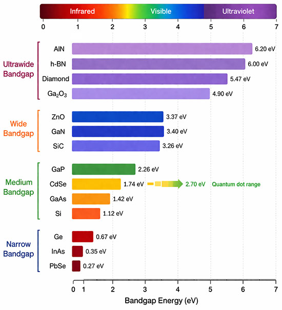
Classification of Bandgap Materials
Narrow-Bandgap Materials
Narrow-bandgap materials have energy gaps below approximately 1 eV. Examples include lead selenide (PbSe), indium arsenide (InAs), and mercury cadmium telluride (HgCdTe). These materials absorb and emit infrared radiation, making them essential for thermal imaging, infrared photodetectors, and thermophotovoltaic energy conversion. At the nanoscale, quantum confinement can widen the bandgap of these materials into the near-infrared or even visible range, expanding their utility far beyond bulk applications.
Medium-Bandgap Materials
Medium-bandgap semiconductors have gaps ranging from about 1 to 2.5 eV and include silicon (Si), germanium (Ge), gallium arsenide (GaAs), cadmium selenide (CdSe), and indium phosphide (InP). Silicon dominates digital electronics and solar cells, while III–V semiconductors like GaAs excel in high-speed electronics, laser diodes, and light-emitting diodes. CdSe quantum dots are among the most widely studied nanomaterials because their emission can be tuned across the entire visible spectrum simply by changing particle size.
Wide-Bandgap Materials
Wide-bandgap (WBG) materials possess energy gaps between approximately 2.5 and 5 eV. Silicon carbide (SiC, ~3.3 eV), gallium nitride (GaN, ~3.4 eV), and zinc oxide (ZnO, ~3.4 eV) are the most prominent members of this class. Their large bandgaps translate into higher breakdown voltages, faster switching speeds, and superior thermal stability compared to silicon. SiC and GaN devices have already entered mass production for power electronics in electric vehicles, renewable energy inverters, and 5G telecommunications infrastructure.
Ultrawide-Bandgap Materials
Ultrawide-bandgap (UWBG) materials have energy gaps exceeding 5 eV and include diamond (~5.5 eV), aluminum nitride (AlN, ~6.2 eV), hexagonal boron nitride (h-BN, ~6.0 eV), and gallium oxide (Ga2O3, ~4.9 eV). These materials promise even higher voltage handling, lower power losses, and operation at extreme temperatures. Diamond, with its exceptional thermal conductivity (2200 W/m·K) and high carrier mobility, is often called the ultimate semiconductor, though practical doping and wafer fabrication remain challenges.
Bandgap Materials at the Nanoscale
At the nanoscale, bandgap materials gain a remarkable property that bulk crystals lack: tunability. When a semiconductor structure shrinks below its exciton Bohr radius – typically a few nanometers – quantum effects confine the electron and hole wavefunctions, discretizing the energy spectrum and widening the bandgap. The dramatically increased surface-to-volume ratio at this scale also modifies electronic states, meaning the same chemical composition can produce different bandgap values depending on particle size, wire diameter, or layer thickness.
This size-dependent tunability is most dramatically demonstrated in quantum dots, where a single material like CdSe can emit light ranging from red to blue as the dot diameter decreases from about 6 nm to 2 nm. Surface states and ligand interactions add another dimension of bandgap control in nanomaterials. In two-dimensional materials like transition metal dichalcogenides, the bandgap can shift by hundreds of millielectron volts between monolayer and few-layer forms – monolayer MoS2, for example, transitions from an indirect gap of 1.29 eV in bulk to a direct gap of 1.89 eV as a single layer.
Key Properties of Bandgap Materials
Electronic Properties
The bandgap determines a material's intrinsic carrier concentration and thus its conductivity at a given temperature. Wide-bandgap materials have far fewer thermally excited carriers, which means lower leakage current and the ability to operate at elevated temperatures without performance degradation. At the nanoscale, quantized energy levels in quantum wires and quantum wells create sharp features in the electronic density of states, enabling precise control over carrier transport in nanoelectronic devices.
Optical Properties
A bandgap material absorbs photons with energies above the gap and is transparent to those below it. This threshold behavior underpins the operation of photodetectors, solar cells, and photonic devices. Direct-bandgap materials like GaAs and InP emit light efficiently through radiative recombination, while indirect-bandgap materials like silicon are poor emitters but can become efficient light sources at the nanoscale when quantum confinement relaxes momentum conservation rules.
Thermal Properties
Wide and ultrawide bandgap materials generally exhibit high thermal conductivity and thermal stability because the large energy gap suppresses thermal generation of carriers. Diamond and SiC, for instance, can operate reliably at temperatures exceeding 300 °C, well beyond the limit of silicon-based devices. These thermal characteristics make wide-bandgap nanomaterials attractive for harsh-environment sensors and power converters.
Catalytic Properties
The bandgap of a photocatalytic material determines which portion of the solar spectrum it can harness. Titanium dioxide (TiO2), a wide-bandgap material at 3.2 eV, absorbs only ultraviolet light, limiting its solar efficiency to about 5% of incident radiation. Bandgap engineering through doping, defect engineering, or heterojunction formation extends the absorption into the visible range, dramatically improving the efficiency of photocatalytic water splitting and pollutant degradation using metal oxide nanoparticles.
Key Applications
Power Electronics and Energy Conversion
Wide-bandgap materials like SiC and GaN are transforming power electronics by enabling smaller, lighter, and more efficient converters. SiC transistors can switch at higher frequencies with lower energy losses, reducing the size of passive components such as inductors and capacitors. Electric vehicle inverters built with SiC devices extend driving range by several percent compared to silicon equivalents, while GaN-based chargers have become standard in compact consumer power adapters.
Displays and Solid-State Lighting
GaN-based LEDs, which exploit the wide bandgap of III–nitride alloys, have made traditional incandescent and fluorescent lighting largely obsolete. By alloying GaN with indium (InGaN) or aluminum (AlGaN), the bandgap can be tuned continuously from the ultraviolet through the entire visible spectrum. Quantum dot films made from semiconductor nanoparticles with precisely tuned bandgaps now serve as color-conversion layers in high-end displays, providing saturated colors with minimal energy loss.
Solar Energy Harvesting
Matching the bandgap of a solar cell absorber to the solar spectrum is critical for maximizing energy conversion. Single-junction cells achieve peak theoretical efficiency with a bandgap near 1.34 eV. Multi-junction architectures stack materials with different bandgaps – such as InGaP (1.86 eV), GaAs (1.42 eV), and germanium (0.67 eV) – to capture a broader range of the spectrum. Quantum dot solar cells and perovskite thin films offer size- and composition-tunable bandgaps as lower-cost alternatives for future photovoltaic technology.
Quantum Technologies
Ultrawide-bandgap materials host atomic-scale defects that function as solid-state quantum emitters. Nitrogen-vacancy centers in diamond and point defects in h-BN and SiC emit single photons on demand and maintain quantum coherence at room temperature. These properties make UWBG materials essential platforms for quantum sensing, quantum communication, and emerging quantum computing architectures that require robust, optically addressable spin states.
Challenges and Future Perspectives
Despite rapid progress, bandgap materials face several obstacles on the path to broader adoption. For wide and ultrawide bandgap semiconductors, achieving reliable p-type doping remains a persistent challenge – GaN, Ga2O3, and diamond all suffer from difficulties in creating acceptor states shallow enough for efficient hole conduction at room temperature. Substrate quality and cost also limit scalability; high-quality SiC and GaN wafers remain considerably more expensive than silicon, though prices have fallen steadily as production volumes increase.
At the nanoscale, controlling the bandgap uniformity of large quantities of quantum dots or nanowires is essential for reproducible device performance. Even sub-nanometer variations in particle diameter can shift emission wavelengths noticeably. Surface traps and atomic vacancies introduce mid-gap states that degrade carrier lifetimes, requiring careful passivation through core–shell architectures or surface functionalization. Computational tools such as density functional theory and machine learning accelerate the identification of promising bandgap materials, but experimental validation of predicted properties often lags behind prediction speed.
Future advances will emerge from the convergence of new material platforms – including MXenes, van der Waals heterostructures, and halide perovskites – with improved synthesis techniques and characterization methods such as electron energy loss spectroscopy. The ability to design bandgap materials with atomic precision, combined with scalable fabrication processes, will unlock applications in flexible electronics, ultra-efficient power systems, deep-ultraviolet photonics, and quantum information technology.
Further Reading
Advanced Electronic Materials, Ultrawide-Bandgap Semiconductors: Research Opportunities and Challenges
Nature Reviews Materials, Bandgap engineering in semiconductor alloy nanomaterials with widely tunable compositions
npj 2D Materials and Applications, Bandgap engineering of two-dimensional semiconductor materials
