-
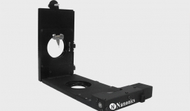
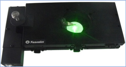
The MultiView 2000TM series is an advanced single probe scanning probe microscope enabling a variety of modes of AFM/SPM/NSOM imaging. Nanonics has designed The MultiView 2000TM for excellence in scanning probe microscopy while allowing for near-field and far-field optical NSOM/AFM Raman/TERS imaging without perturbation. The Multiview 2000TM is the only commercially available instrument that offers both tip and sample scanning. This versatility is important for different operation modes where the user can now choose whether the sample or tip is static. The Multiview 2000TM further offers the most stable feedback mechanism available in the form of normal force feedback with tuning fork actuation. This feedback mechanism offers the most stability, as well as laser-free operation for the most sensitive experiments. -

Nanonics Imaging Ltd. provides near-field optical microscopes (NSOM or SNOM) and atomic force microscopes (AFM). The company offers photonics and plasmonics, defect analysis solutions, dual optical microscopes, scanning stages, and scanned probe microscopy (SPM) probes and nanotools. It also provides NSOM and SPM accessories, such as liquid cells, environmental chamber and nanochemical/gas delivery systems, vibration isolation platforms, APD controllers, double APD detection systems, and NSOM and SPM heads for customized sample stages. The company’s SPM and NSOM systems comprise NSOM (SNOM) systems for transmission, collection, and true reflection NSOM imaging; Raman systems; tip-and sample-scanning probe systems for AFM/Raman/tip enhanced Raman spectroscopy and NSOM/ANSOM applications; photonics/plasmonics workstations that are designed to address nano/micro photonic characterization; fountain pen nanolithography package for chemical writing of liquids and gases; and integrated SPM with electron and ion beam microscopes. Its products are used in chemical sciences, lens characterization, life sciences, microelectronics, nanochemistry, photonics and telecommunication, physics, polymers, Raman, semiconductors, and TFT display applications. Nanonics Imaging Ltd. was founded in 1997 and is headquartered in Jerusalem, Israel.
Visit company website
The contents of this site are copyright ©2005-2024 Nanowerk. All Rights Reserved.