Nanowerk Catalog
Bruker Atomic Force Microscopes (AFM) and other nano technologies incorporate the very latest advances in AFM techniques, including the revolutionary PeakForce Tapping to ideally suit a wide array of application areas, from biology to semiconductors, from data storage devices to polymers, and from integrated optics to measurement of forces between particles and surfaces.
Bruker 3D metrology and inspection systems include 3D Optical Microscopes and Stylus Profilers. These deliver high speed automated measurements of critical dimensions, roughness, flatness and form. Applications include QA/QC on medical devices, tribology, film thickness, trench depths and optics form and finish. Our new production software enables fully automated one button operation. Instruments range from cost effective benchtop R&D systems to standalone high throughput production tools.
Bruker Tribological Tools and Mechanical Testing tools incorporate innovative, leading-edge technologies — including proprietary multi-sensing technology with high-sample-rate data-acquisition hardware & software, highest-accuracy force sensors and amplifiers, high-frequency acoustic emission sensors and amplifiers, and more.
Bruker Fluorescence Microscopy Products provide leading optical instrument designs and rich software features to researchers in neurobiology and cell biology for conducting uncaging experiments, optogenetics, simultaneous electrophysiology studies, as well as photoactivation, photostimulation and photoablation experiments.
Products listed on Nanowerk
No content yet.
No content yet.
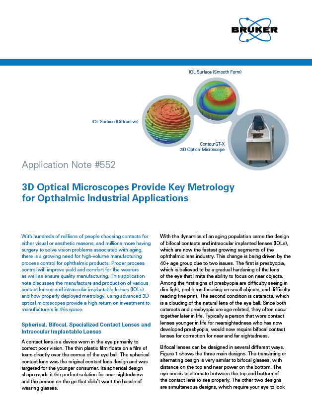
3D Optical Microscopes Provide Key Metrology for Opthalmic Industrial Applications
With hundreds of millions of people wearing contacts, and millions more having surgery to solve vision problems associated with aging, there is a gro...
3D Optical Microscopes Provide Key Metrology for Opthalmic Industrial Applications Details
-
- With hundreds of millions of people wearing contacts, and millions more having surgery to solve vision problems associated with aging, there is a growing need for high-volume manufacturing process control for ophthalmic products. This application note discusses the manufacture and production of various contact lenses and intraocular implantable lenses and how properly deployed metrology, using advanced 3D optical microscopes provide a high return on investment to manufacturers.
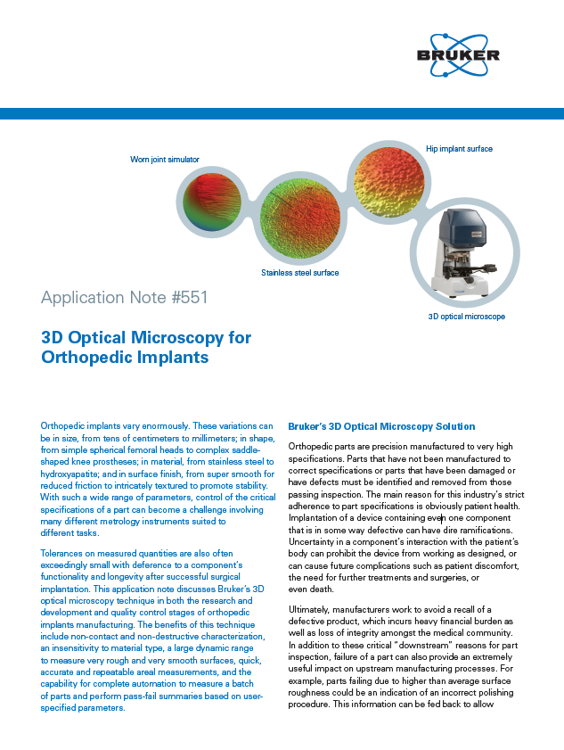
3D Optical Microscopy for Orthopedic Implants
This application note discusses the use of 3D optical microscopy in the R&D and quality control stages of orthopedic implants manufacturing. The bene...
3D Optical Microscopy for Orthopedic Implants Details
-
- This application note discusses the use of 3D optical microscopy in the R&D and quality control stages of orthopedic implants manufacturing. The benefits of this technique include non-contact/non-destructive characterization; an insensitivity to material type; a large dynamic range to measure very rough and very smooth surfaces, quick accurate and repeatable areal measurements; and automation to measure a batch of parts and perform pass-fail summaries based on user-specified parameters.
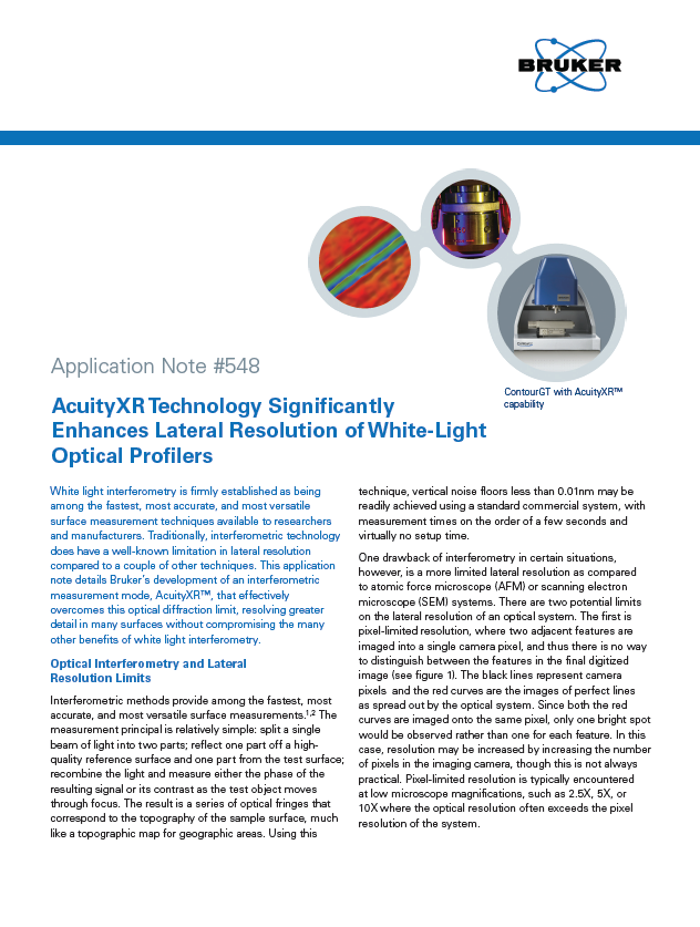
AcuityXR Technology Significantly Enhances Lateral Resolution of White-Light Optical Profilers
White light interferometry (WLI) is among the fastest, most accurate, and most versatile surface measurement techniques available. Traditionally, inte...
AcuityXR Technology Significantly Enhances Lateral Resolution of White-Light Optical Profilers Details
-
- White light interferometry (WLI) is among the fastest, most accurate, and most versatile surface measurement techniques available. Traditionally, interferometric technology does have a well-known limitation in lateral resolution compared to a couple of other techniques. This application note details an interferometric measurement mode, AcuityXR™, that effectively overcomes this optical diffraction limit, resolving greater detail in many surfaces without compromising the many other benefits WLI.
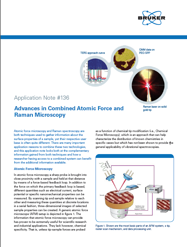
Advances in Combined Atomic Force and Raman Microscopy
Atomic force microscopy and Raman spectroscopy are both techniques used to gather information about the surface properties of a sample, yet their resp...
Advances in Combined Atomic Force and Raman Microscopy Details
-
- Atomic force microscopy and Raman spectroscopy are both techniques used to gather information about the surface properties of a sample, yet their respective user base is often quite different. There are many important application reasons to combine these two technologies, and this application note looks both at the complementary information gained from both techniques and how a researcher having access to a combined system can benefit from the additional information available.
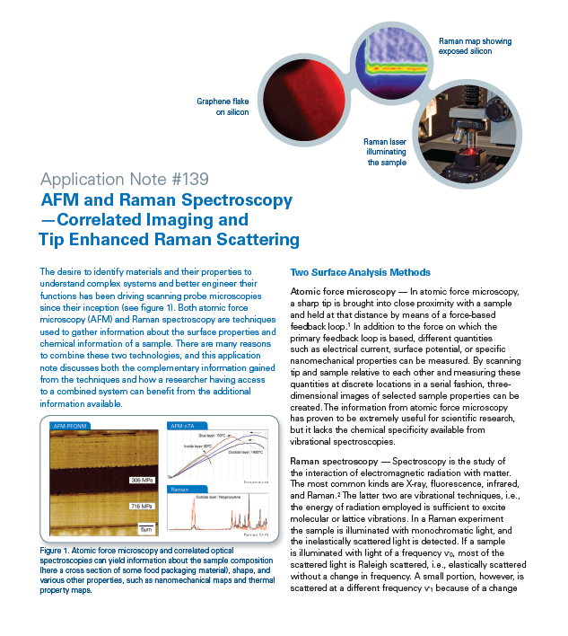
AFM and Raman Spectroscopy —Correlated Imaging and Tip Enhanced Raman Scattering
The desire to identify materials and their properties to understand complex systems and better engineer their functions has been driving scanning prob...
AFM and Raman Spectroscopy —Correlated Imaging and Tip Enhanced Raman Scattering Details
-
- The desire to identify materials and their properties to understand complex systems and better engineer their functions has been driving scanning probe microscopies since their inception. Both AFM and Raman spectroscopy are techniques used to gather information about the surface properties and chemical information of a sample. There are many reasons to combine these two technologies, and this application note discusses the complementary information gained from the techniques.
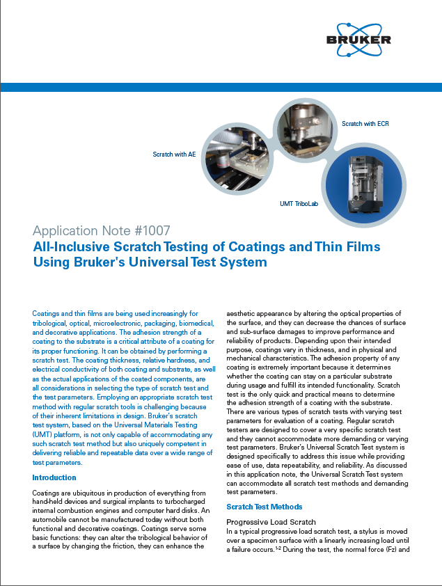
All-Inclusive Scratch Testing of Coatings and Thin Films Using Bruker's Universal Test System
The adhesion strength of a coating to the substrate is a critical attribute of a coating for its proper functioning. This application note discusses h...
All-Inclusive Scratch Testing of Coatings and Thin Films Using Bruker's Universal Test System Details
-
- The adhesion strength of a coating to the substrate is a critical attribute of a coating for its proper functioning. This application note discusses how the coating thickness, relative hardness, and electrical conductivity of both coating and substrate, as well as the actual applications of the coated components, are all considerations in selecting the type of scratch test and the test parameters. The UMT TriboLab's is uniquely capable of accommodating any such scratch test method.
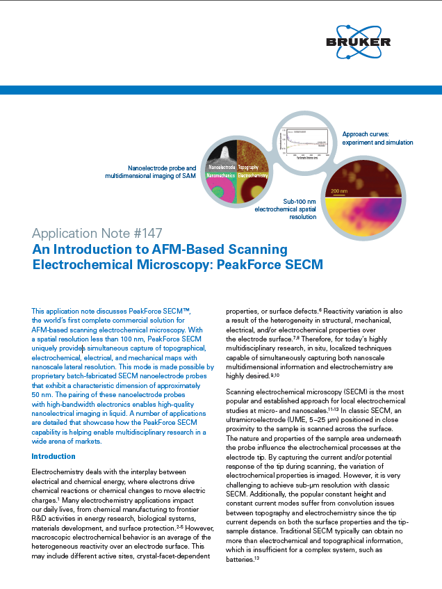
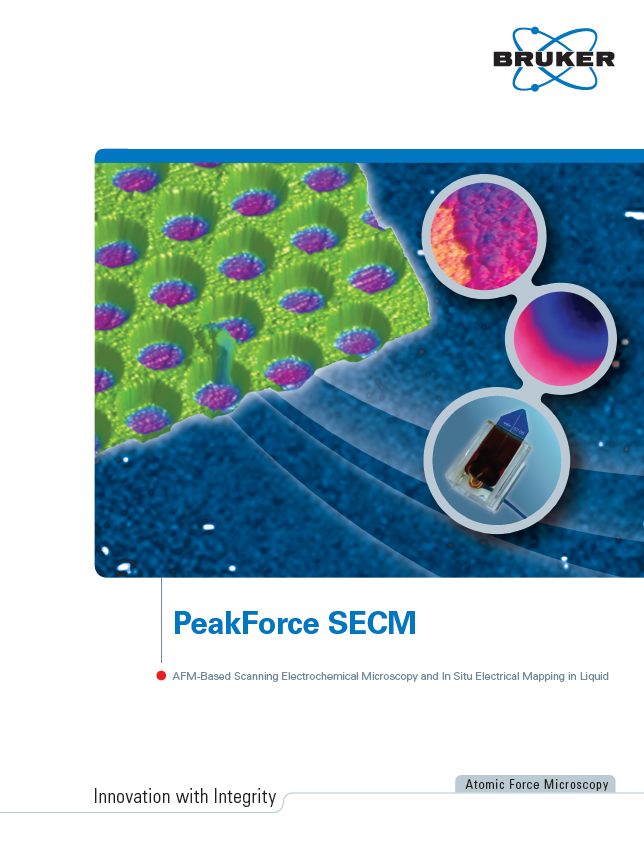
An Introduction to AFM-Based Scanning Electrochemical Microscopy: PeakForce SECM
This application note discusses PeakForce SECM™, the world’s first complete commercial solution for AFM-based scanning electrochemical microscopy....
An Introduction to AFM-Based Scanning Electrochemical Microscopy: PeakForce SECM Details
-
- This application note discusses PeakForce SECM™, the world’s first complete commercial solution for AFM-based scanning electrochemical microscopy. With a spatial resolution less than 100 nm, PeakForce SECM uniquely provides simultaneous capture of topographical, electrochemical, electrical, and mechanical maps with nanoscale lateral resolution. A number of applications are detailed that showcase how the technique is helping enable multidisciplinary research in a wide range of markets.
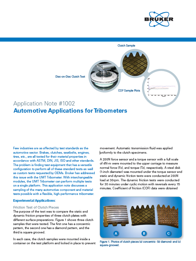
Automotive Applications for Tribometers
In the automotive industry, brakes, clutches, seatbelts, engines, tires, etc., are all tested for their material properties in accordance with ASTM, D...
Automotive Applications for Tribometers Details
-
- In the automotive industry, brakes, clutches, seatbelts, engines, tires, etc., are all tested for their material properties in accordance with ASTM, DIN, JIS, ISO and other standards. The problem is finding test equipment to perform all of these standard tests as well as custom tests requested by OEMs. This application note discusses a sampling of the many automotive component and material tests possible with a flexible, high-performance tribometer.
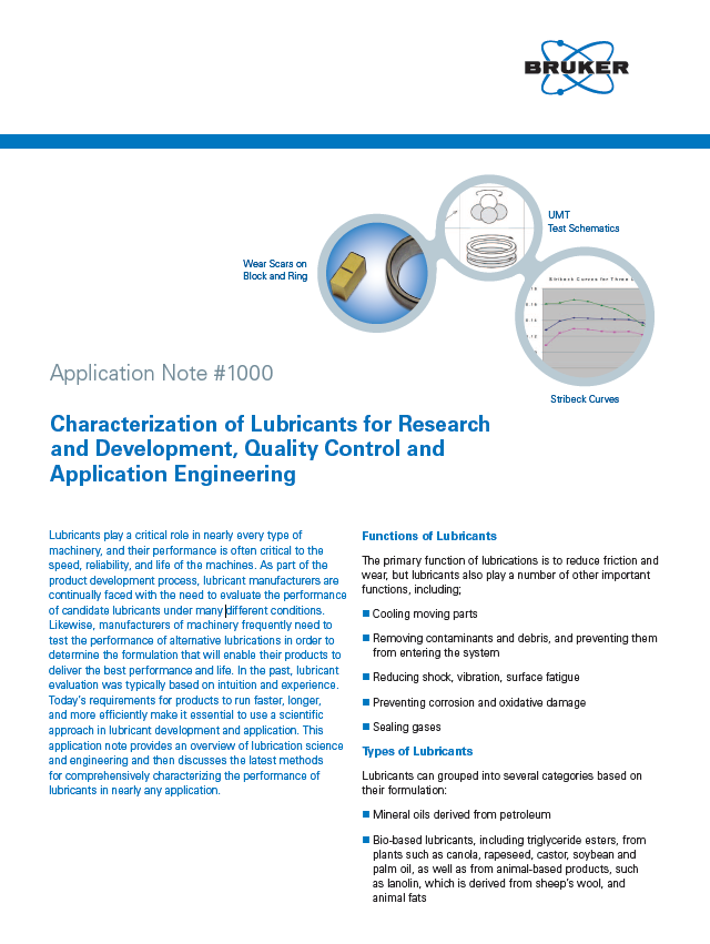
Characterization of Lubricants for Research and Development, Quality Control and Application Engineering
Lubricants play a critical role in nearly every type of machinery, and their performance is often critical to the speed, reliability, and life of the ...
Characterization of Lubricants for Research and Development, Quality Control and Application Engineering Details
-
- Lubricants play a critical role in nearly every type of machinery, and their performance is often critical to the speed, reliability, and life of the machines. For products to run faster, longer, and more efficiently a scientific approach in lubricant development is required. This application note provides an overview of lubrication science and engineering and discusses the latest methods for comprehensively characterizing the performance of lubricants in nearly any application.
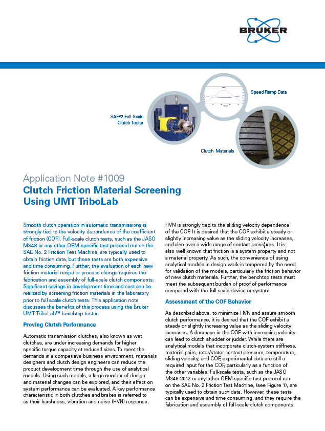
Clutch Friction Material Screening Using UMT TriboLab
Smooth clutch operation in automatic transmissions is strongly tied to the velocity dependence of the coefficient of friction. Full-scale clutch tests...
Clutch Friction Material Screening Using UMT TriboLab Details
-
- Smooth clutch operation in automatic transmissions is strongly tied to the velocity dependence of the coefficient of friction. Full-scale clutch tests are typically used to obtain friction data, but these tests are both expensive and time consuming. Significant savings in development time and cost can be realized by screening friction materials in the laboratory prior to full-scale clutch tests. This application note discusses the benefits of this process using the UMT TriboLab benchtop tester.
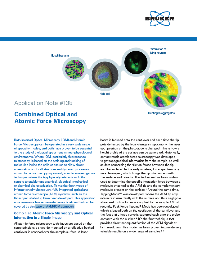
Combined Optical and Atomic Force Microscopy
Both Inverted Optical Microscopy (IOM) and Atomic Force Microscopy can be operated in a very wide range of specialty modes, and both have proven to be...
Combined Optical and Atomic Force Microscopy Details
-
- Both Inverted Optical Microscopy (IOM) and Atomic Force Microscopy can be operated in a very wide range of specialty modes, and both have proven to be essential to the study of biological specimens in near-physiological environments. To monitor both types of information simultaneously, fully integrated optical and AFM systems have been developed. This application note reviews a few representative applications that can be covered by this type of AFM/IOM approach.
Common Approaches to Tip Functionalization for AFM-Based Molecular Recognition Measurements

AFM has been widely used to measure the nanomechanical properties of materials ranging from polymers to living cells and even to characterize single m...
Common Approaches to Tip Functionalization for AFM-Based Molecular Recognition Measurements Details
-
- AFM has been widely used to measure the nanomechanical properties of materials ranging from polymers to living cells and even to characterize single molecules. These measurements are normally made using common, unmodified AFM probes. However, another type of measurement is made possible by the chemical functionalization of AFM probes. This technical note reviews common approaches to functionalizing AFM tips for this type of research.
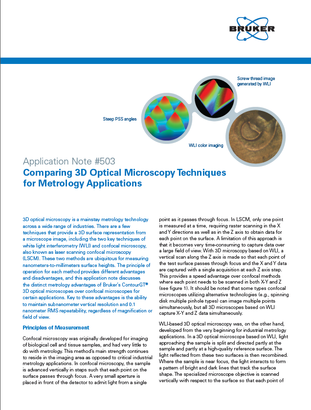
Comparing 3D Optical Microscopy Techniques for Metrology Applications
There are a few techniques that provide a 3D surface representation from a microscope image, including the two key techniques of white light interfero...
Comparing 3D Optical Microscopy Techniques for Metrology Applications Details
-
- There are a few techniques that provide a 3D surface representation from a microscope image, including the two key techniques of white light interferometry and confocal microscopy, also known as laser scanning confocal microscopy. The principle of operation for each method provides different advantages and disadvantages, and this application note discusses the distinct metrology advantages of 3D optical microscopes over confocal microscopes for certain applications.
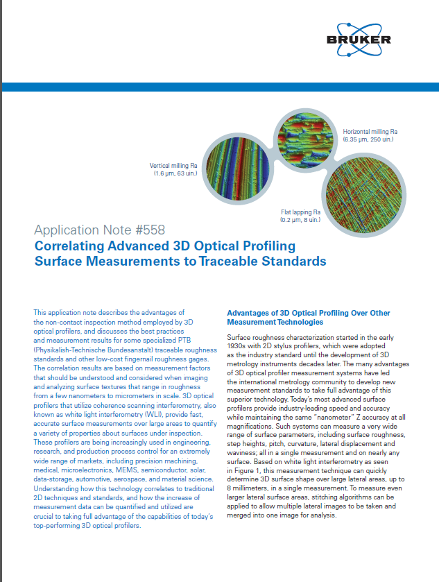
Correlating Advanced 3D Optical Profiling Surface Measurements to Traceable Standards
This application note describes the advantages of the non-contact inspection method employed by 3D optical profilers, and discusses the best practices...
Correlating Advanced 3D Optical Profiling Surface Measurements to Traceable Standards Details
-
- This application note describes the advantages of the non-contact inspection method employed by 3D optical profilers, and discusses the best practices and measurement results for some specialized PTB (Physikalish-Technische Bundesanstalt) traceable roughness standards and other low-cost fingernail roughness gages.
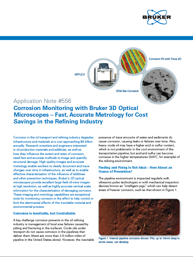
Corrosion Monitoring with Bruker 3D Optical Microscopes – Fast, Accurate Metrology for Cost Savings in the Refining Industry
Research scientists and engineers interested in oil production materials and additives, as well as how they influence the extent and rates of corrosi...
Corrosion Monitoring with Bruker 3D Optical Microscopes – Fast, Accurate Metrology for Cost Savings in the Refining Industry Details
-
- Research scientists and engineers interested in oil production materials and additives, as well as how they influence the extent and rates of corrosion, need fast and accurate methods to image and quantify structural damage. This application note discusses how 3D optical microscopes provide excellent large field-of-view images at high resolution, as well as highly accurate vertical scale information for the characterization of damaging corrosion.
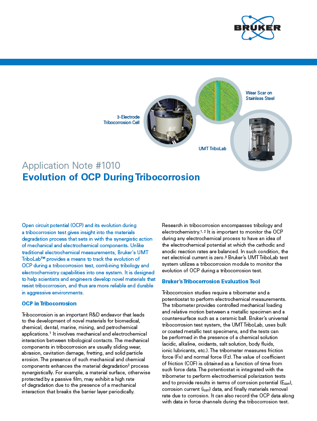
Evolution of OCP During Tribocorrosion
Open circuit potential (OCP) and its evolution during a tribocorrosion test gives insight into the materials degradation process that sets in with the...
Evolution of OCP During Tribocorrosion Details
-
- Open circuit potential (OCP) and its evolution during a tribocorrosion test gives insight into the materials degradation process that sets in with the synergistic action of mechanical and electrochemical components. This application note discusses how UMT TriboLab™ provides a means to track the evolution of OCP during a tribocorrosion test, combining tribology and electrochemistry capabilities into one system, helping engineers develop novel materials that resist tribocorrosion.
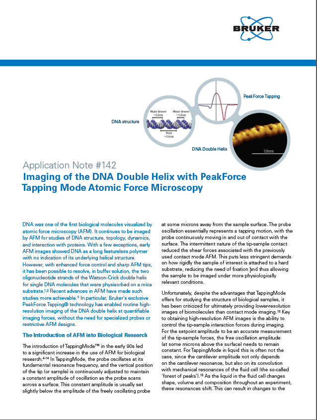
Imaging of the DNA Double Helix with PeakForce Tapping Mode Atomic Force Microscopy
Recent advances in AFM have made the study of DNA structures more achievable. This application note discusses how Bruker’s exclusive PeakForce Tappi...
Imaging of the DNA Double Helix with PeakForce Tapping Mode Atomic Force Microscopy Details
-
- Recent advances in AFM have made the study of DNA structures more achievable. This application note discusses how Bruker’s exclusive PeakForce Tapping® technology has enabled routine high-resolution imaging of the DNA double helix at quantifiable imaging forces, without the need for specialized probes or restrictive AFM designs.
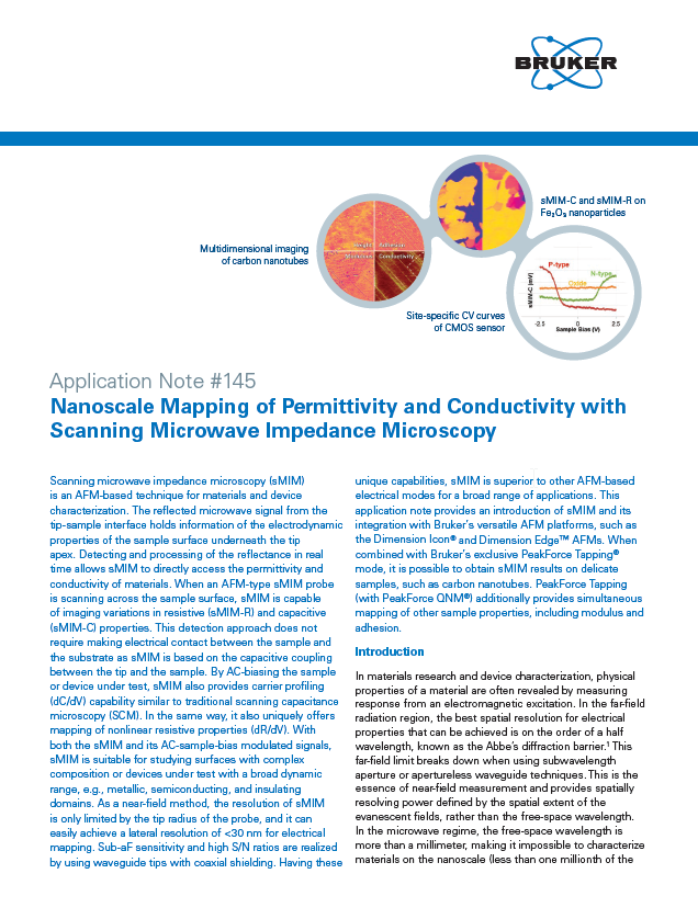
Nanoscale Mapping of Permittivity and Conductivity with Scanning Microwave Impedance Microscopy
Scanning microwave impedance microscopy (sMIM) is an AFM-based technique for materials and device characterization. This application note provides an ...
Nanoscale Mapping of Permittivity and Conductivity with Scanning Microwave Impedance Microscopy Details
-
- Scanning microwave impedance microscopy (sMIM) is an AFM-based technique for materials and device characterization. This application note provides an introduction of sMIM. When combined with Bruker’s exclusive PeakForce Tapping® mode, it is possible to obtain sMIM results on delicate samples, such as carbon nanotubes.
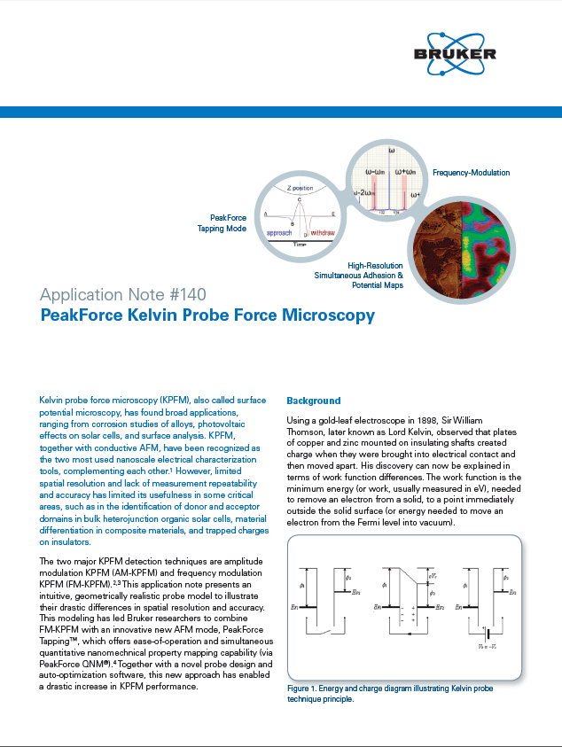
PeakForce Kelvin Probe Force Microscopy
Kelvin probe force microscopy (KPFM), also called surface potential microscopy, has found broad applications, ranging from corrosion studies of alloys...
PeakForce Kelvin Probe Force Microscopy Details
-
- Kelvin probe force microscopy (KPFM), also called surface potential microscopy, has found broad applications, ranging from corrosion studies of alloys, photovoltaic effects on solar cells, and surface analysis. KPFM, together with conductive AFM, have been recognized as the two most used nanoscale electrical characterization tools, complementing each other. This application note discusses Bruker's suite of new KPFM modes, three of which are based on breakthrough PeakForce Tapping technology.
PeakForce SECM brochure
Bruker’s exclusive PeakForce SECM™ mode is the world’s first complete commercial solution for AFM-based scanning electrochemical microscopy (SEC...
PeakForce SECM brochure Details
-
- Bruker’s exclusive PeakForce SECM™ mode is the world’s first complete commercial solution for AFM-based scanning electrochemical microscopy (SECM) with a spatial resolution less than 100 nanometers. Utilizing an innovative probe design, AFM-based SECM with nanoscale resolution is now widely available for emerging research on chemistry kinetics, biochemical signaling and environmental chemistry.
PeakForce Tapping brochure
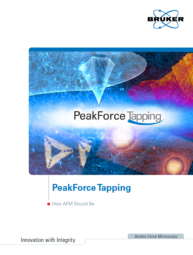
Bruker’s exclusive PeakForce Tapping® is the most significant scientific breakthrough in atomic force microscope (AFM) technology since the introdu...
PeakForce Tapping brochure Details
-
- Bruker’s exclusive PeakForce Tapping® is the most significant scientific breakthrough in atomic force microscope (AFM) technology since the introduction of TappingMode™. It provides unprecedented high-resolution imaging, extends AFM measurements into a range of samples not previously accessed and uniquely enables simultaneous nanoscale property mapping.
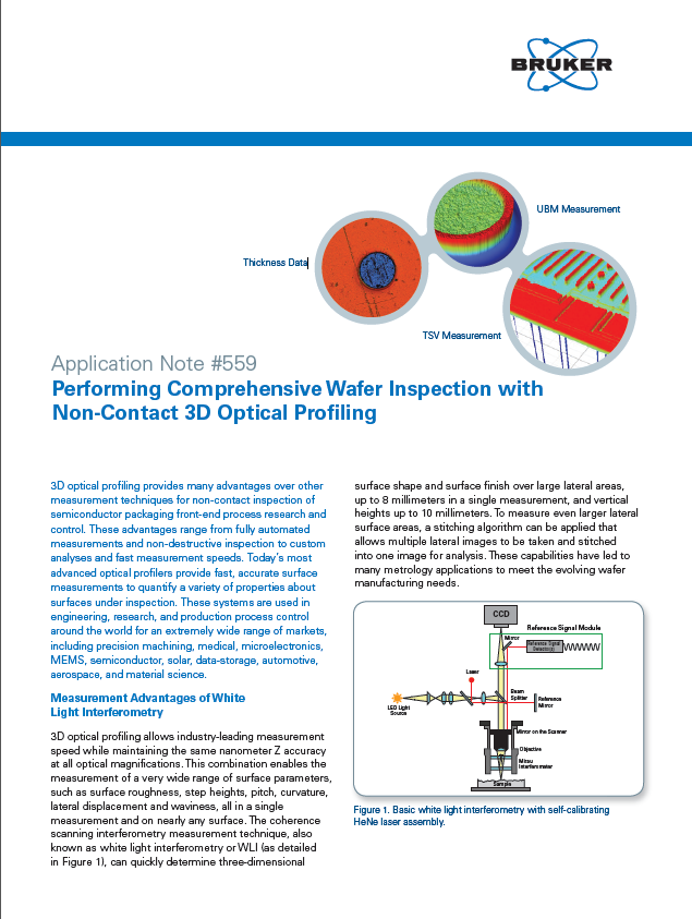
Performing Comprehensive Wafer Inspection with Non-Contact 3D Optical Profiling
3D optical profiling provides many advantages over other measurement techniques for non-contact inspection of semiconductor packaging front-end proces...
Performing Comprehensive Wafer Inspection with Non-Contact 3D Optical Profiling Details
-
- 3D optical profiling provides many advantages over other measurement techniques for non-contact inspection of semiconductor packaging front-end process research and control. This application note discusses how these advantages range from fully automated measurements and non-destructive inspection to custom analyses and fast measurement speeds. Today’s most advanced optical profilers provide fast, accurate surface measurements to quantify a variety of properties about surfaces under inspection.
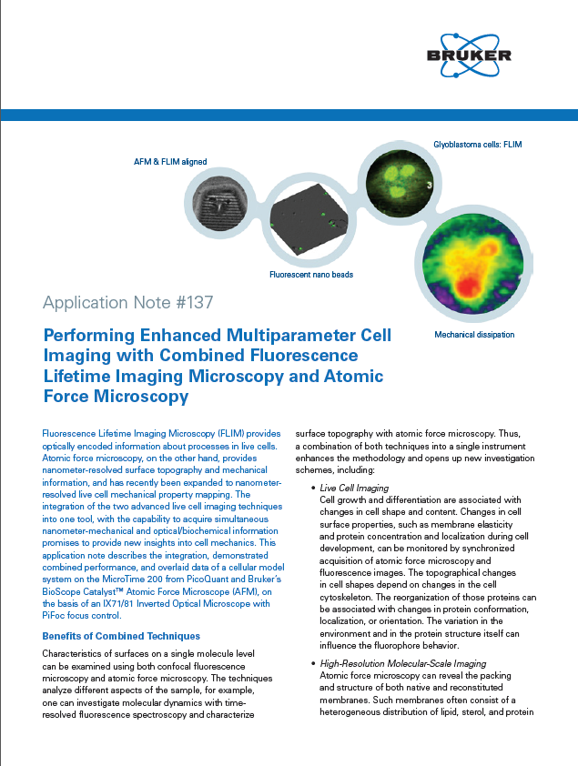
Performing Enhanced Multiparameter Cell Imaging with Combined Fluorescence Lifetime Imaging Microscopy and Atomic Force Microscopy
Fluorescence Lifetime Imaging Microscopy (FLIM) provides optically encoded information about processes in live cells. Atomic force microscopy provides...
Performing Enhanced Multiparameter Cell Imaging with Combined Fluorescence Lifetime Imaging Microscopy and Atomic Force Microscopy Details
-
- Fluorescence Lifetime Imaging Microscopy (FLIM) provides optically encoded information about processes in live cells. Atomic force microscopy provides nanometer-resolved surface topography and mechanical information. This application note discusse integration of the two techniques into one tool, with the capability to acquire simultaneous nanometer-mechanical and optical/biochemical information to provide new insights into cell mechanics.
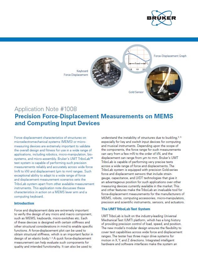
Precision Force-Displacement Measurements on MEMS and Computing Input Devices
Force-displacement characteristics of structures on microelectromechanical systems (MEMS) or micromeasuring devices are extremely important to validat...
Precision Force-Displacement Measurements on MEMS and Computing Input Devices Details
-
- Force-displacement characteristics of structures on microelectromechanical systems (MEMS) or micromeasuring devices are extremely important to validate the overall design and fitness for use in a wide range of applications, including robotics, micro-manipulation, biosystems, and micro-assembly. This application note discusses performing such precision measurements reliably and accurately on a MEMS lever arm and a computing keyboard across wide force (mN to kN) and displacement (μm to mm) ranges.
Quantitative Imaging of Living Biological Samples by PeakForce QNM Atomic Force Microscopy
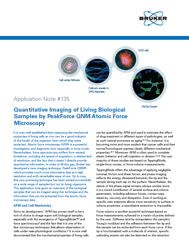
Force spectroscopy suffers from several limitations in studying living cells, including the speed of acquisition, a relative lack of resolution, and ...
Quantitative Imaging of Living Biological Samples by PeakForce QNM Atomic Force Microscopy Details
-
- Force spectroscopy suffers from several limitations in studying living cells, including the speed of acquisition, a relative lack of resolution, and a lack of quantitative information. PeakForce QNM® provides much more informative data at a high resolution with remarkable ease-of-use. This application note gives an overview of the biological samples that can be imaged using this technique and the information that can be extracted from the atomic force microscopy data.
Quantitative Mechanical Property Mapping at the Nanoscale with PeakForce QNM
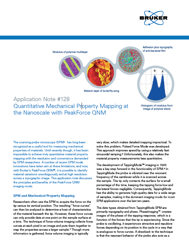
Until relatively recently SPM has not been able to achieve truly quantitative material property mapping with high resolution. With PeakForce QNM® it ...
Quantitative Mechanical Property Mapping at the Nanoscale with PeakForce QNM Details
-
- Until relatively recently SPM has not been able to achieve truly quantitative material property mapping with high resolution. With PeakForce QNM® it is possible to identify material variations unambiguously and at high resolution across a topographic image. This application note discusses the principles and benefits of the PeakForce QNM imaging mode.
Simultaneous Electrical and Mechanical Property Mapping at the Nanoscale with PeakForce TUNA
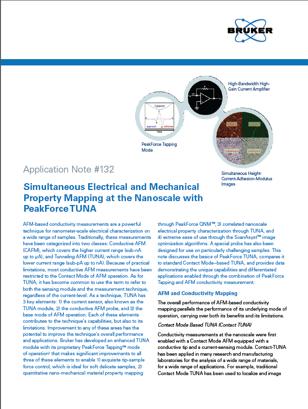
This application note discusses the basics of PeakForce TUNA, compares it to standard Contact Mode–based TUNA, and provides data demonstrating the u...
Simultaneous Electrical and Mechanical Property Mapping at the Nanoscale with PeakForce TUNA Details
-
- This application note discusses the basics of PeakForce TUNA, compares it to standard Contact Mode–based TUNA, and provides data demonstrating the unique capabilities and differentiated applications enabled through the combination of PeakForce Tapping and AFM conductivity measurement.
Survey, Screening, Dynamics: A No-Compromise Approach to High-Speed Atomic Force Microscopy
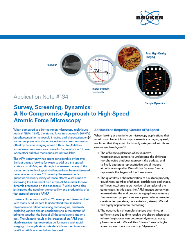
The AFM community has spent considerable effort over the last decade looking for ways to address the speed limitation of AFMs. Bruker’s development ...
Survey, Screening, Dynamics: A No-Compromise Approach to High-Speed Atomic Force Microscopy Details
-
- The AFM community has spent considerable effort over the last decade looking for ways to address the speed limitation of AFMs. Bruker’s development team worked with many AFM leaders, iteratively exploring various design considerations in the pursuit of bringing together the best of all these solutions into one tool. This application note details how the Dimension FastScan ideally marries high-resolution performance with rapid imaging.
Thin Film and Coating Testing Using Bruker‘s UMT Testers
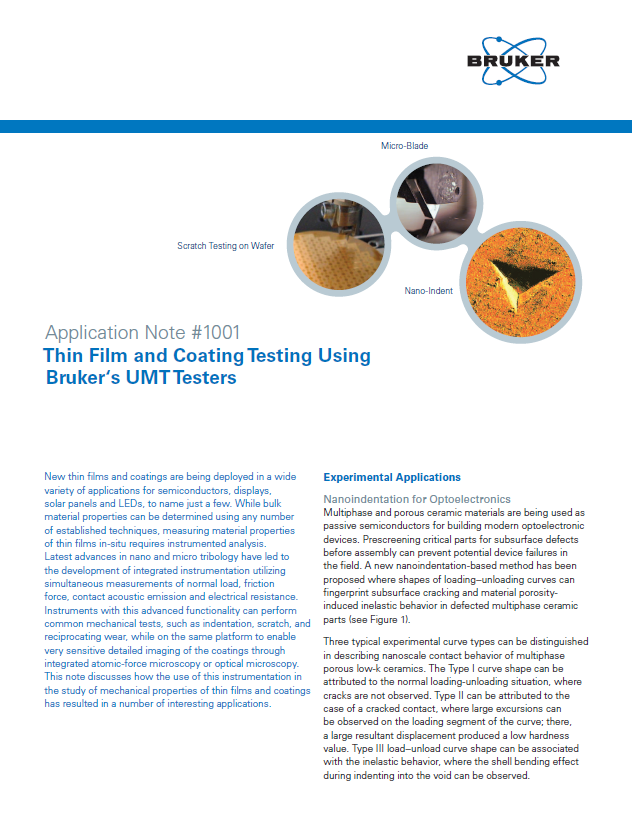
New thin films and coatings are being deployed in a wide variety of applications for semiconductors, displays, solar panels and LEDs. This application...
Thin Film and Coating Testing Using Bruker‘s UMT Testers Details
-
- New thin films and coatings are being deployed in a wide variety of applications for semiconductors, displays, solar panels and LEDs. This application note discusses how the latest advances in nano and micro tribology have led to the development of integrated instrumentation utilizing simultaneous measurements of normal load, friction force, contact acoustic emission and electrical resistance, resulting in a number of interesting applications.
Toward Quantitative Nanomechanical Measurements on Live Cells with PeakForce QNM
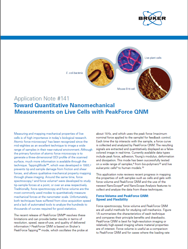
Measuring and mapping mechanical properties of live cells is of high importance in today’s biological research. This application note reviews the ca...
Toward Quantitative Nanomechanical Measurements on Live Cells with PeakForce QNM Details
-
- Measuring and mapping mechanical properties of live cells is of high importance in today’s biological research. This application note reviews the capabilities of BioScope Resolve to map the properties of soft samples, including live cells and gels, with force volume and PeakForce QNM modes. It also demonstrates features of the NanoScope Analysis software to collect and analyze the data from these techniques.
Understanding Engine Tribology: Performing Reciprocating Tests of a Piston Ring's Interaction with the Cylinder Liner
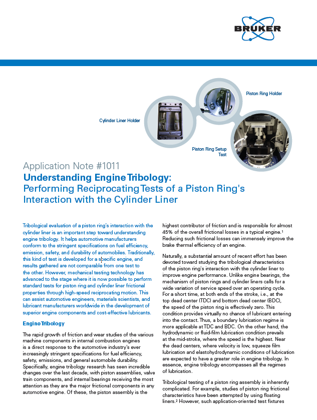
Tribological evaluation of a piston ring’s interaction with the cylinder liner helps automotive manufacturers conform to the stringent specification...
Understanding Engine Tribology: Performing Reciprocating Tests of a Piston Ring's Interaction with the Cylinder Liner Details
-
- Tribological evaluation of a piston ring’s interaction with the cylinder liner helps automotive manufacturers conform to the stringent specifications on fuel efficiency, emission, safety, and durability of automobiles. This application note discusses how mechanical testing technology has advanced to the stage where it is now possible to perform standard tests for piston ring and cylinder liner frictional properties through high-speed reciprocating motion.
Using the UMT TriboLab and Stribeck Curves to Evaluate Potential Applications of Lubricants
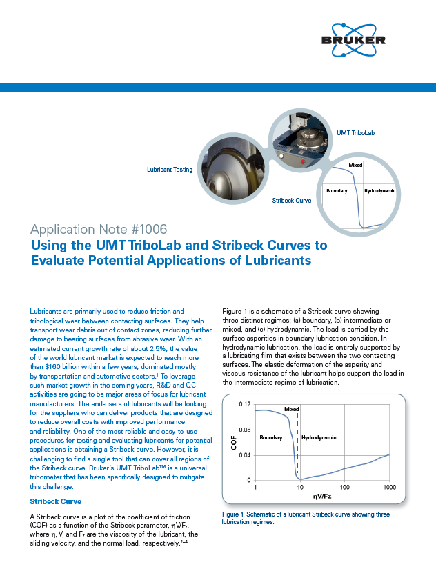
End-users of lubricants look for suppliers who can deliver products designed to reduce overall costs with improved performance and reliability. One of...
Using the UMT TriboLab and Stribeck Curves to Evaluate Potential Applications of Lubricants Details
-
- End-users of lubricants look for suppliers who can deliver products designed to reduce overall costs with improved performance and reliability. One of the most reliable and easy-to-use procedures for testing and evaluating lubricants for potential applications is obtaining a Stribeck curve. However, it is challenging to find a single tool that can cover all regions of the Stribeck curve. UMT TriboLab is a universal tribometer that has been specifically designed to mitigate this challenge.
Vision64 Map brochure
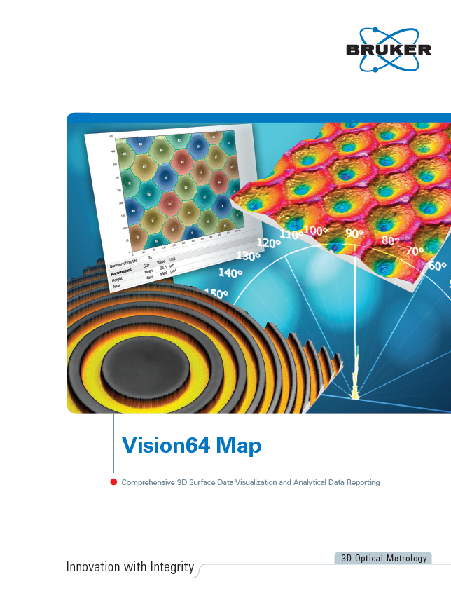
Vision64 Map™ data analysis and reporting software, based on Digital Surf’s industry-leading Mountains® Technology, is a comprehensive extension...
Vision64 Map brochure Details
-
- Vision64 Map™ data analysis and reporting software, based on Digital Surf’s industry-leading Mountains® Technology, is a comprehensive extension to Bruker’s Vision64® instrument control and analysis software. Vision64 Map enables more comprehensive 3D surface visualization and analysis with Bruker 3D optical microscope systems. Now, a complete metrology workflow is available for users, from automated data acquisition and advanced data analysis to powerful data visualization and reporting.
VITA: Quantitative Nanoscale Characterization and Unambiguous Material Identification for Polymers
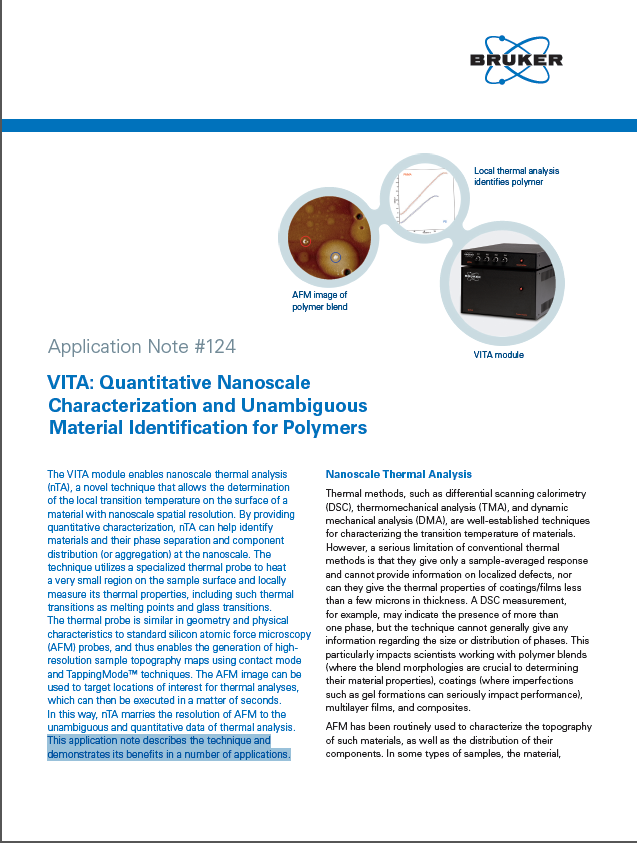
The VITA module enables nanoscale thermal analysis (nTA), a novel technique that allows the determination of the local transition temperature on the s...
VITA: Quantitative Nanoscale Characterization and Unambiguous Material Identification for Polymers Details
-
- The VITA module enables nanoscale thermal analysis (nTA), a novel technique that allows the determination of the local transition temperature on the surface of a material with nanoscale spatial resolution. By providing quantitative characterization, nTA can help identify materials and their phase separation and component distribution (or aggregation) at the nanoscale. This application note describes the VITA technique and demonstrates its benefits in a number of applications.
VXI Universal Surface Measurements for 3D Optical Microscopes
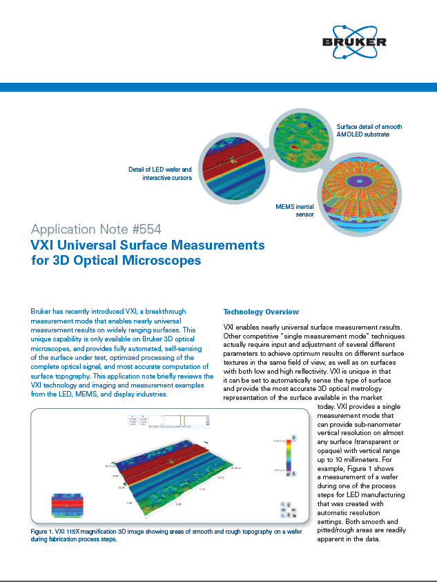
Bruker's VXI is a breakthrough measurement mode that enables nearly universal measurement results on widely ranging surfaces. This unique capability ...
VXI Universal Surface Measurements for 3D Optical Microscopes Details
-
- Bruker's VXI is a breakthrough measurement mode that enables nearly universal measurement results on widely ranging surfaces. This unique capability provides fully automated, self-sensing of the surface under test, optimized processing of the complete optical signal, and most accurate computation of surface topography. This application note briefly reviews the VXI technology and imaging and measurement examples from the LED, MEMS, and display industries.
-
Advancements in Optical Profiler Technology: From Wyko NT to Contour Elite | Bruker Webinar


-
AFMBIOMED Conference Overview

-
Bench Top Screening of Wet Clutch Materials | Bruker Webinar

-
Contour Elite Automation Applications

-
Dektak XTL Automation

-
Hysitron PI 95 Series | Bruker

-
Introduction to the Bruker UMT TriboLab | Bruker

-
PeakForce Scanning Electrochemical Measurement | Bruker Webinar

-
Technology Advances in Nanomechanics | Bruker Webinar


The contents of this site are copyright ©2005-2024 Nanowerk. All Rights Reserved.