The Fuel Cell Nano-Materials Group at International Center for Materials Nanoarchitectonics has successfully developed two types of novel proton conducting oxide electrolytes for solid oxide fuel cells (SOFCs). By applying these electrolytes, the commercialization of SOFCs operating in the intermediate temperature range, 500C to 650C, has come into sight.
Nov 22nd, 2010
Read more
Purdue University has been awarded $1.5 million to study quantum information science, a new field paving the way for quantum computing - a novel method to process information that is faster, more powerful and more efficient than classical computing.
Nov 21st, 2010
Read more
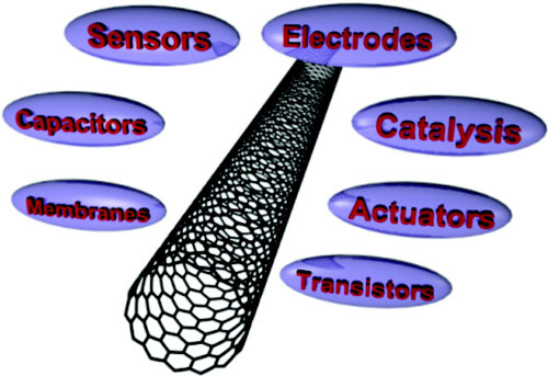 Jan M. Schnorr and Timothy M. Swager from the Department of Chemistry and Institute for Soldier Nanotechnologies at MIT have published an overview of a variety of applications that are based on the unique properties of pristine as well as functionalized carbon nanotubes.
Nov 21st, 2010
Read more
Researchers from the Department of Cell Biology, Physiology and Immunology at Universitat Autonoma de Barcelona (UAB), in collaboration with researchers from the Institute of Microelectronics of Barcelona (IMB-CNM) of the Spanish National Research Council (CSIC), have developed an identification system for oocytes and embryos in which each can be individually tagged using silicon barcodes.
Nov 19th, 2010
Read more
 Atherosclerosis is characterized by hardening and thickening of artery walls, with serious health consequences. Researchers at TU/e have imaged the stages in the calcification at a nanometer scale. The growth of hardening follows almost the same process as bone or tooth formation.
Nov 19th, 2010
Read more
The University of Dayton School of Engineering has hired two faculty members with a combined nine inventions for the region's Wright Brothers Institute and the state's Ohio Research Scholars program to help create technologies that could lead to jobs.
Nov 19th, 2010
Read more
Researchers at BYU have created a micro device that could both decrease the amount of blood and time needed to test for cancer-markers in a patient's blood.
Nov 19th, 2010
Read more
Not long after Dr. Ali Dhinojwala, chairman of The University of Akron Department of Polymer Science, unpeeled the secret (fine, clingy hairs) behind the remarkable adhesion of gecko feet, he and fellow researchers came up with a synthetic replica: carbon nanotubes. Now, five years after that initial discovery, they have published the basis of the success of these nanotubes.
Nov 19th, 2010
Read more
Applications are now invited from UK companies to participate in NanoMission Japan 2011 which will allow companies the opportunity to participate in the major international event Nano Tech Japan 2011 held annually in Tokyo. The Exhibition will run from 16th-18th February 2011.
Nov 19th, 2010
Read more
 HZB-Forscher koennen kleinste Zellbestandteile in ihrer natuerlichen Umgebung sichtbar machen - die Zelle bleibt intakt.
Nov 19th, 2010
Read more
We are surrounded by nanoelectronics through products such as computers, mobile phones, sensors and electric cars. Nanoelectronics may also grow much stronger in the energy efficiency area in the near future. However, the sustainable growth faces several challenges.
Nov 19th, 2010
Read more
A*STAR's Institute of Materials Research and Engineering (IMRE) partners 10 EU research organisations to work on the groundbreaking EUR10 million ATMOL project that lays the foundation for creating and testing a molecular-sized processor chip.
Nov 19th, 2010
Read more
ASU faculty member co-edits the second volume in the series Yearbook of Nanotechnology in Society that explores the significant impact new technologies can have on personal, national and global equity.
Nov 18th, 2010
Read more
 Heisenberg Uncertainty Principle sets limits on Einstein's 'spooky action at a distance,' new research finds.
Nov 18th, 2010
Read more
Wiley-VCH today announced the launch of the journal Advanced Energy Materials, a new international scientific journal dedicated to publishing high impact research in energy-related materials.
Nov 18th, 2010
Read more
Researchers at ORNL are developing a method of packing more circuitry into a smaller space on these silicon wafers. Referred to as 100-nanometer lithography, the term reflects the feature resolution required to pack extremely tiny circuits directly onto the microchip wafers. Recent improvements in optical lithography, however, have pushed the requirements for next-generation lithography closer to 70- or 50-nanometer feature size.
Nov 18th, 2010
Read more
 Subscribe to our Nanotechnology News feed