The Foresight Institute, a nanotechnology education and public policy think tank based in Palo Alto, has announced the winners of the prestigious 2010 Foresight Institute Feynman Prizes in Nanotechnology.
Dec 20th, 2010
Read more
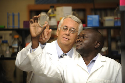 The National Institutes of Health has designated Auburn University's College of Veterinary Medicine a Center for Translational Cancer Nanomedicine. The five-year, $1.7 million award is part of a larger, $13.5 million grant from the NIH National Cancer Institute which established a Center for Cancer Nanotechnology Excellence.
Dec 18th, 2010
Read more
Australia's National Industrial Notification and Assessment Scheme (NICNAS) has issued guidance on new chemical requirements for the notification of industrial nanomaterials. The notification and assessment process comes in effect on January 1, 2011.
Dec 18th, 2010
Read more
 A new European access centre called ACTMOST will provide European companies with timely, cost-effective, and investment-free access to professional, cutting-edge micro-photonic technologies and knowledge to support the development of new products.
Dec 18th, 2010
Read more
Imec has demonstrated the selective area growth of high-quality InP layers on 200mm Si(001) wafers. Key to avoiding the typically formed and unwanted antiphase boundaries (APBs) is the creation of atomic steps on a thin Ge buffer layer. This result is a major step forward towards the fabrication of high-performance Ge/III-V CMOS devices and the integration of optoelectronic devices on a Si chip.
Dec 18th, 2010
Read more
 The joint European project SEAL (Semiconductor Equipment Assessment Leveraging Innovation), dedicated to foster the European semiconductor equipment industry in a global market has been successfully started.
Dec 18th, 2010
Read more
Researchers from imec and the University of Michigan have reported a new technology to fabricate complex three-dimensional microstructures, with intricate bends, twists, and multidirectional textures, starting from vertically aligned carbon nanotubes.
Dec 18th, 2010
Read more
Imec has derived a process flow concept for the packaging of medical implants that meets the requirements for miniaturization, biocompatibility and safety. The proposed solution is a promising alternative for the currently used rigid packages that tend to enhance foreign body reactions.
Dec 18th, 2010
Read more
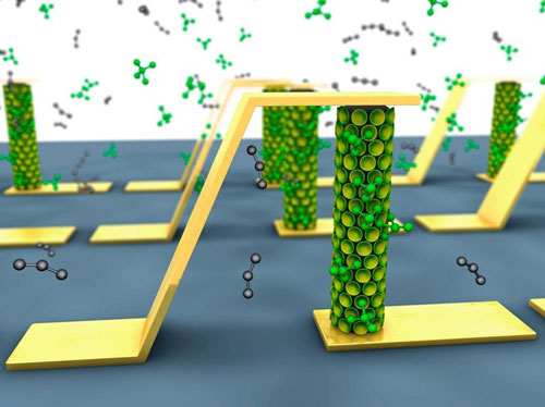 Imec and Holst Centre have developed an innovative sensor for measuring ultra-low concentrations of NO2. Such sensors are important for applications that monitor environmental pollution resulting from traffic, and in general, from all combustion motors. The sensor's active components are arrays of grown vertical InAs nanowires.
Dec 18th, 2010
Read more
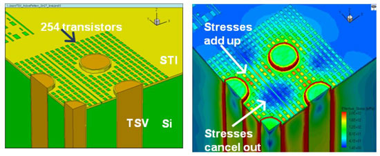 At IEDM 2010, imec and its partners presented a study of the stress-induced impact of through-silicon via (TSV) processing on the performance of high-k/metal-gate CMOS transistors and circuits. This study is a first of its kind; the results and the approach that was followed are a foundation for stress-aware design with dedicated design rules. This will allow to precisely delineate keep-out zones, and thus to save valuable silicon area.
Dec 18th, 2010
Read more
Researchers at the Nottingham Nanotechnology and Nanoscience Center etch a tiny periodic table onto a hair.
Dec 18th, 2010
Read more
 Researchers at Eindhoven University of Technology and the COBRA research institute in Eindhoven have succeeded in causing electron transport using an electronic 'ratchet'. This is the first time that usable powers have been generated at room temperature with a device of this kind. The finding opens the possibility of a new kind of wireless drive for microelectronic circuits.
Dec 17th, 2010
Read more
Researchers at Brown University and in Korea have described the dynamics behind cutting single-walled carbon nanotubes, cylindrical structures just 1/50,000th the width of a human hair. The tubes are compressed by potent sonic booms, causing them to buckle at certain points at helical, 90-degree angles. The finding could lead to better-quality nanotubes for potential use in automotive, electronics, optics and other fields.
Dec 17th, 2010
Read more
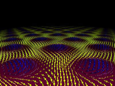 Physicists set a lattice of magnetic vortices in a material in motion using electric current almost a million times weaker than in earlier studies.
Dec 17th, 2010
Read more
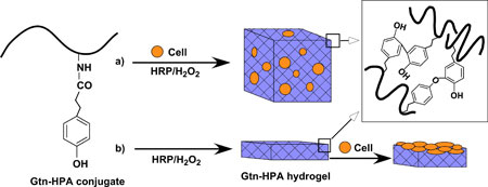 Scientists at the Institute of Bioengineering and Nanotechnology (IBN), the world's first bioengineering and nanotechnology research institute, have developed the first injectable hydrogel system with variable stiffness that can control cell proliferation and differentiation in a two-dimensional (2D) and three-dimensional (3D) cell culture environment.
Dec 17th, 2010
Read more
 Mathematical equations can now resolve whether electron transport in nanostructures follows classical or quantum mechanical behavior.
Dec 17th, 2010
Read more
 Subscribe to our Nanotechnology News feed