The solar cell that also shines: Luminescent 'LED-type' design breaks efficiency record
 Research to be presented at the Conference on Lasers and Electro Optics illuminates 50-year mystery.
Apr 19th, 2012
Read moreResearch to be presented at the Conference on Lasers and Electro Optics illuminates 50-year mystery.
Apr 19th, 2012
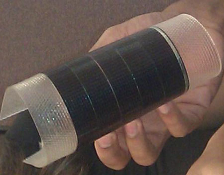
Read moreA new prototype reveals that a layer of graphene, when strained through stretching, can act as a two-dimensional lens for electrons.
Apr 19th, 2012
Read more Harnessing the energy of sunlight can be as simple as tuning the optical and electronic properties of metal oxides at the atomic level by making an artificial crystal or super-lattice 'sandwich'.
Apr 19th, 2012
Read more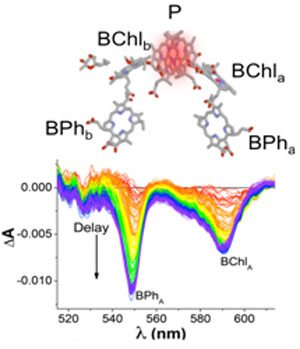 Across billions of years of evolution, Nature has retained a common light-absorbing hexameric cofactor core for carrying out the very first chemical reaction of photosynthesis, the light-induced electron transfer across approximately 3 nm. This process has direct analogies to light-driven charge separation in photovoltaic devices.
Apr 19th, 2012
Read moreResearchers from the NIST Center for Nanoscale Science and Technology and Massachusetts Institute of Technology have used the scanning electron microscopy with polarization analysis (SEMPA) technique to provide the first direct images of the magnetic structure of highly twisted domain walls in patterned thin film magnetic nanowires.
Apr 19th, 2012
Read more Nanoscale films developed at MIT promote bone growth, creating a stronger seal between implants and patients' own bone.
Apr 19th, 2012
Read more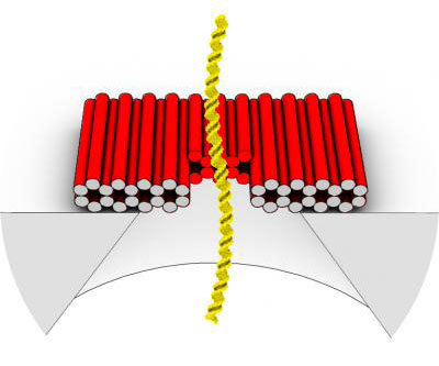 Two advances combine for new capabilities in single-molecule sensing.
Apr 19th, 2012
Read more New research at Concordia University is bringing us one step closer to clean energy. It is possible to extend the length of time a battery-like enzyme can store energy from seconds to hours.
Apr 18th, 2012
Read moreA team of researchers from Taiwan and the University of California, Berkeley, has harnessed nanodots to create a new electronic memory technology that can write and erase data 10-100 times faster than today's mainstream charge-storage memory products.
Apr 18th, 2012
Read more'Organic and large-area electronics' (OLAE) is focused on materials and devices built from organic carbon-based molecules that are able to conduct electricity. Because these are lighter, more flexible and less expensive than inorganic conductors, such as copper or silicon, they are a viable alternative for many electronics applications.
Apr 18th, 2012
Read more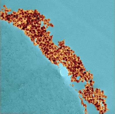 Cotton is going high-tech in New Orleans, La., where a team of U.S. Department of Agriculture (USDA) scientists is continuing a long tradition of innovative research on the prized natural fiber.
Apr 18th, 2012
Read moreAmerican Associates, Ben-Gurion University of the Negev (AABGU) just received a $3 million pledge from long-time AABGU supporter and National Vice President Ruth Flinkman-Marandy and Ben Marandy. This generous donation will support a new atom chip and quantum optics research and development facility at Ben-Gurion University of the Negev in Beer-Sheva, Israel.
Apr 18th, 2012
Read moreMedicine-toting nanochains slip into tumors and explode a chemotherapy drug into hard-to-reach cores of cancer, engineers and scientists at Case Western Reserve University report.
Apr 18th, 2012
Read more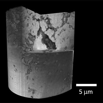 A new x-ray microscope probes the inner intricacies of materials smaller than human cells and creates unparalleled high-resolution 3D images.
Apr 18th, 2012
Read moreThe eBeam Initiative, a forum dedicated to the education and promotion of new semiconductor manufacturing approaches based on electron beam (eBeam) technologies, today announced that several of its members will present the latest breakthroughs using eBeam technologies to improve photomask critical dimension uniformity (CDU) and wafer yields this week during Photomask Japan (PMJ) 2012, the 19th international symposium on photomasks and nextgeneration lithography masks being held at the Pacifico Yokohama in Yokohama, Japan.
Apr 18th, 2012
Read more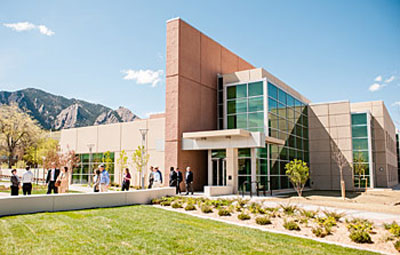 Two new advanced laboratory buildings for high-precision science and measurements have officially opened in Boulder, Colo., providing upgraded facilities to support technology innovation and economic growth as well as the training of future scientists.
Apr 18th, 2012
Read more Subscribe to our Nanotechnology News feed