| Posted: May 22, 2006 | |
Fabricating three dimensional nanostructures using two photon lithography in a single exposure step |
|
| (Nanowerk Spotlight) New research shows that soft, conformable sub-wavelength phase masks can be used, with 2-photon effects, to pattern in a parallel fashion and in a single exposure step large, 3D structures in certain classes of photopolymers. The result is a technique that is simple from an experimental standpoint, but which fully exploits the flexibility and patterning capabilities enabled by 2-photon effects, making it useful for applications in photonics, microfluidics and biotechnology. | |
| Scientists at the Rogers Research Group at the University of Illinois at Urbana-Campaign have been working on low cost soft lithographic approaches to fabricating 3D nanostructures in ways that are scalable to large areas. By adjusting the polarization and coherence of the light sources, and by engineering specific geometries into the masks, they were able to demonstrate a wide range of capabilities for 3D patterning. | |
| In a recent paper, titled "Fabricating three dimensional nanostructures using two photon lithography in a single exposure step" Professor Rogers and his group, together with Gary Wiederrecht from Argonne National Laboratory presents a parallel, large area route to 3D nanostructures by two photon patterning in thick transparent photopolymers. | |
| Seokwoo Jeon, first author of the paper, explains the novelty of their findings to Nanowerk: "Our approach enables 2-photon lithography to be performed in a completely parallel fashion, which is in sharp contrast to conventional 2-photon methods that involve the serial scanning of a focused laser beam to 'write' 3D structures. The parallel operation of our method increases fabrication speeds and scalability to areas, by many orders of magnitude." | |
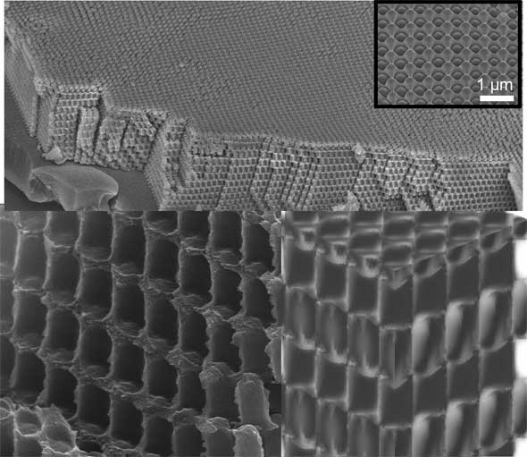 | |
| SEM images and modeling of 3D structures made through a two photon process with mask 1 (a) large area angled view and top view (inset) and (b) cross sectional view (left) and modeling (right). An appropriately defined cutoff filter, close to the experimental condition, is chosen for modeling. (Source: Seokwoo Jeon, University of Illinois at Urbana-Campaign) | |
| Compared to conventional interference lithography, this work is the first demonstration of full 3D pattering with 2-photon effect. In 2-photon lithography, very high peak intensities are required. To achieve such intensities, short pulsed lasers are used. | |
| The problem with the use of such light sources in conventional methods (i.e. interference lithography) is that any combination of multiple beams of light from these pulsed lasers requires extremely precise alignment and control to ensure spatial and temporal overlap of the pulses (which have very short spatial and temporal durations). | |
| "In our approach" says Jeon, "we expose the 2-photon sensitive photopolymer directly in proximity to the surface of conformable masks that generates a 3D distribution of intensity. Separate manipulation of beams and pulse overlaps is not required. In this way, we bypass the difficulties associated with using 2-photon lithography in the conventional manner." | |
| "However, even though we build 3D structures in parallel fashion, the required peak pulse energy is still very high" says Jeon. | |
| To make 3D structures in large area with higher speed, the design of more sensitive 2-photon photopolymer is a key challenge to be overcome. Higher sensitivity would also allow to use a longer pulse, so that the depth of 3D structures can be increased in proportion to that. | |
| "The modeling is doable and we have the capabilities, but it is not trivial" says Jeon. "We do full vector modeling of the optics to determine, for a given mask, the distribution of intensity near its surface and, therefore, the geometry of the 3D structures that we can produce. We are currently working on a more powerful modeling tool that would allow us to solve the inverse problem, i.e. to determine how one can generate a phase mask to produce a desired 3D structure. With this type of tool we will be able to more fully exploit the power of this patterning approach." | |
 By
Michael
Berger
– Michael is author of three books by the Royal Society of Chemistry:
Nano-Society: Pushing the Boundaries of Technology,
Nanotechnology: The Future is Tiny, and
Nanoengineering: The Skills and Tools Making Technology Invisible
Copyright ©
Nanowerk LLC
By
Michael
Berger
– Michael is author of three books by the Royal Society of Chemistry:
Nano-Society: Pushing the Boundaries of Technology,
Nanotechnology: The Future is Tiny, and
Nanoengineering: The Skills and Tools Making Technology Invisible
Copyright ©
Nanowerk LLC
|
Become a Spotlight guest author! Join our large and growing group of guest contributors. Have you just published a scientific paper or have other exciting developments to share with the nanotechnology community? Here is how to publish on nanowerk.com.