| Posted: Jun 28, 2012 | |
Mass production of high quality graphene: An analysis of worldwide patents |
|
| (Nanowerk Spotlight) Graphene (read more: What is graphene?) is undoubtedly emerging as the most promising nanomaterial because of its unique combination of superb properties, which opens a way for its exploitation in a wide spectrum of applications. However, it has to overcome a number of obstacles before we can realize its full potential for practical applications. | |
| One of the greatest challenges being faced today in commercializing graphene is how to produce high quality material, on a large scale at low cost, and in a reproducible manner. | |
| The quality of graphene plays a crucial role as the presence of defects, impurities, grain boundaries, multiple domains, structural disorders, wrinkles in the graphene sheet can have an adverse effect on its electronic and optical properties. In electronic applications, the major bottleneck is the requirement of large size samples, which is possible only in the case of CVD process, but it is difficult to produce high quality and single crystalline graphene thin films possessing very high electrical and thermal conductivities along with excellent optical transparency. | |
| Another issue of concern in the synthesis of graphene by conventional methods involves the use of toxic chemicals and these methods usually result in the generation hazardous waste and poisonous gases. Therefore, there is a need to develop green methods to produce graphene by following environmentally friendly approaches. The preparation methods for graphene should also allow for in-situ fabrication and integration of graphene-based devices with complex architecture that would enable eliminating the multi step and laborious fabrication methods at a lower production cost. | |
| The major hurdle in manufacturing graphene on an industrial scale is the process complexity and the associated high cost of its production, which results in expensive product. For example, currently, the selling prices of 50x50 monolayer graphene thin films by Graphene Square are $263 and $819 on Cu foil and PET thin film, respectively. Graphene nanoplatelets (5-8 nm thick) manufactured by XG Sciences is sold at about $219-229/ kg. The high cost of graphene is one of the major obstacles to its widespread adoption for commercial applications. | |
| Nevertheless, it is expected that the market for graphene would grow by leaps and bounds in the coming decade. According to the latest report “Graphene: Technologies, Applications and Markets” released by BCC the global graphene market is projected to grow to $67 million in 2015 and $675.1 by 2020 at a Compound Average Annual Growth Rate (CAGR) of 58.7% within a period of 5 years. Another report entitled "world market for graphene to 2017" by the future markets, Inc. 2011 estimates that the production volume of graphene in 2010 was 28 tonnes and is projected to grow to 573 Tonnes by 2017. | |
| In the present article, an attempt has been made to carry out an extensive survey and analysis of global patents pertaining to the various processes of graphene synthesis. The article initially summarizes the current status of the conventional approaches for the synthesis of graphene based on the survey of literature. There are several good reviews available on the subject 1-7 and the interested readers may like to refer to the same for obtaining further details. The article particularly focuses on large-scale production methods for making high quality graphene. | |
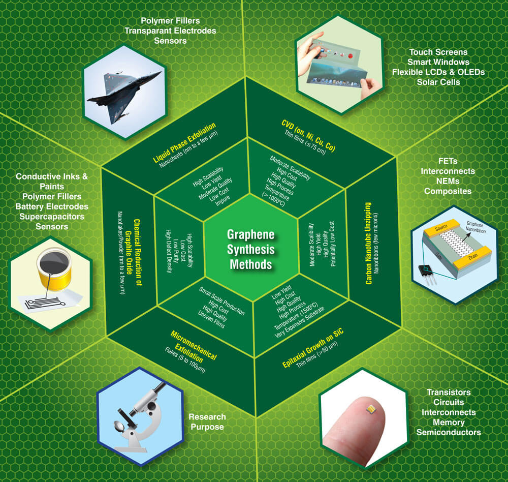
| Currently, the most common techniques available for the production of graphene are shown schematically in Fig. 1, which includes micromechanical cleavage, chemical vapour deposition, epitaxial growth on SiC substrates, chemical reduction of exfoliated graphene oxide, liquid phase exfoliation of graphite and unzipping of carbon nanotubes. However, each of the above methods can have its own advantages as well as limitations depending on its target application(s) as depicted in Fig. 1. In order to surmount these barriers in commercializing graphene, concerted efforts are being made by researchers at various R&D institutes, universities and companies from all over the globe to develop new methods for large scale production of low-cost and high quality graphene via simple and eco-friendly approaches. | |
 |
|
| Fig. 1: A shematic showing the conventional methods commonly used for the synthesis of graphene along with their key features, and the current and future applications. (Image: CKMNT) (click image to enlarge) | |
| Patent analysis | |
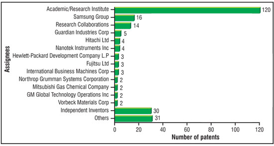
| Efforts have been made to identify the key players actively pursuing R&D activity in the rapidly emerging area of graphene synthesis. As shown in the bar chart of Fig. 2, the analysis reveals that academic/research institutes from all over the globe are doing a significant amount of research and hold the lion’s share of patents (120 patents), i.e. about 50% of the total patents filed worldwide. The second category among the assignees leading the patenting activity is independent inventors (30 patents), out of which, Jang Bor Z from Wright State University has filed 25 patents. Fig. 2 also shows that Samsung Group is the world leader with 16 patents to its credit followed by a number of companies, including Guardian Industries Corp., Hitachi Ltd., Nanotek Instruments, Hewlett Packard Development Co., L.P., Fujitsu Ltd., IBM Corp etc. | |
 |
|
| Fig. 2: Assignee-wise segmentation of patents related to graphene synthesis. (Image: CKMNT) | |
| In view of the major intellectual property (I.P) contributions made by the academic/research institutes to the field of graphene synthesis, it would be pertinent to take a closer look at their role in this activity. | |
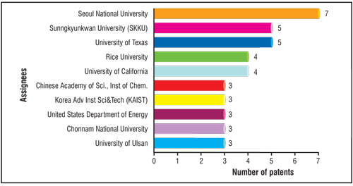
| The number of patents owned by the top ten academic/research institutes is given in the bar chart of Fig. 3, and it is evident that Seoul National University followed by Sunngkyunkwan University (SKKU), both from South Korea are the most active assignees with 7 and 5 patents to their credit, respectively. Other active assignees are University of Texas (5 patents), Rice University (4 patents) and University of California (4 patents) all from USA. Other major players in this category are Chinese Academy of Sciences- Institute of Chemistry, China, Korea Advanced Institute of Science and Technology (KAIST), Korea, US Department of Energy, USA, Chonnam National University and Kyung Hee University, Korea. It is noteworthy that among the top ten, six universities belong to South Korea alone. | |
 |
|
| Fig. 3: Number of patents related to grapheme synthesis for the top 10 academic/research institutes. (Image: CKMNT) | |
| Graphene Synthesis Methods | |
| In view of the immense potential of graphene for commercial and strategic applications, scientists from all over the world are intensively pursuing research and development activities to develop a variety of techniques for its synthesis, as evidenced by the large number of scientific publications and patents that have appeared in recent years. Of course, the focus has been on large-scale production of high quality graphene at low cost. Currently, innumerable techniques are available for the preparation of graphene. However, one can broadly classify them into two main categories, i.e. bottom-up (e.g., CVD, epitaxial growth on SiC, arc discharge, chemical synthesis etc.) and top-down (e.g., exfoliation methods) processes. | |
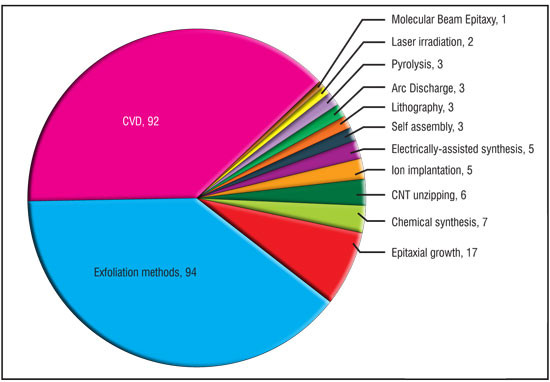
| Synthesis of graphene has been classified according to the techniques employed by analysing the filed, published and granted patents. Based on this analysis (Fig. 4) it is quite evident that substantial patenting activity is directed towards the development of CVD (92 patents) and exfoliation (94 patents) techniques. Although it is not shown in the pie chart of Fig. 4, it may be noted that exfoliation methods mainly include 1) mechanical exfoliation of graphite, 2) liquid phase exfoliation of graphite and 3) chemical exfoliation of graphite oxide. Other dominant techniques are epitaxial growth on SiC substrates (17 patents), chemical synthesis (7 patents) and unzipping of carbon nanotubes (6 patents). All the above mentioned methods have significant potential for scaled-up production of graphene at an affordable cost. The pie chart also shows other emerging techniques like ion implantation, electrochemical deposition, arc discharge, self assembly, laser irradiation etc. | |
 |
|
| Fig. 4: Segmentation of graphene synthesis methods. (Image: CKMNT) | |
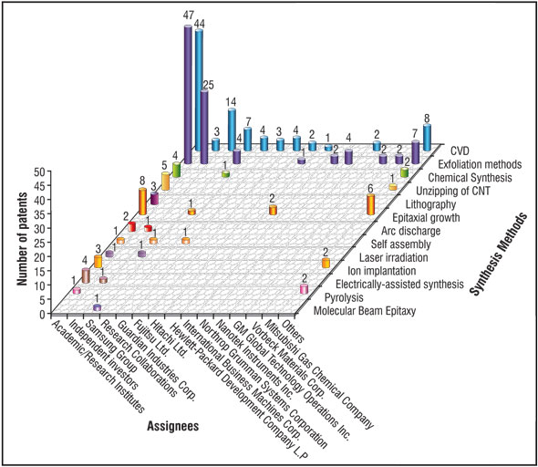
| The data was analysed and is presented as a three-dimensional graph in Fig. 5 for each of the top patent assignees against the synthesis methods. | |
| It is interesting to note that most of the multinational corporations such as Samsung Group, IBM, Hitachi Ltd. etc. are following the CVD approach to develop high-end electronic or optoelectronic products based on high quality large area graphene thin films. | |
| In contrast, the start-up companies such as Nanotech Instruments (Angstron Materials), XG Sciences, Vorbeck Materials Corp. are directing their efforts towards developing processing routes like exfoliation, chemical synthesis, etc. for the large scale production of graphene nanoplatelets used for low-end products, e.g., fillers for plastics, battery and supercapacitor electrodes, conductive inks and coatings etc. Academic/research institutes are focussing on developing diverse approaches like electrochemical exfoliation, microwave-assisted synthesis, liquid phase exfoliation, chemical synthesis, CVD and so forth. Some of the key players making significant contributions to this research field are Seoul National University and Korea Institute of Science and Technology (CVD), University of Ulsan, Chonnam National University (Exfoliation technique); Beijing Institute of Technology and Institute of Physics, Chinese Academy of Sciences (Epitaxial growth); National Nanomaterials and University of Idaho (Chemical synthesis); Stanford Junior University and Rice University (Unzipping of CNTs) and so on. | |
 |
|
| Fig. 5: Segmentation of patents related to synthesis methods and the assignees. (Image: CKMNT) (click on image to enlarge) | |
| Innovative Approaches for the Large Scale Production of High Quality Graphene | |
| As we have discussed earlier, graphene offers numerous opportunities for commercial exploitation because of its limitless potential for applications such as ultra strong and tough composites, touch screens, energy storage, ultra-fast transistors and so on. However, to realize its true potential for real life applications one needs to produce it in large quantities at an affordable cost, and depending on each application one has to tailor it in a suitable form and required quality. In order to meet these challenges, all-out efforts are being made by the worldwide scientific community to develop innovative approaches for the production of graphene. Some of the emerging routes for the synthesis of graphene along with the active players are introduced below. | |
| Chemical Vapor Deposition (CVD) for Electronic and Optoelectronic Devices | |
| Graphene is an ideal candidate for the manufacture of the next generation miniaturised, lightweight, ultra-fast and high frequency electronic and optoelectronic devices. The quality of the graphene is of paramount importance for these applications and for this purpose one has to produce large area graphene monolayer or few layer thin films of ultimate purity, large domain size, and uniform thickness. Moreover, the material should be free of any defects, grain boundaries, structural disorder, and wrinkles. CVD route has the potential to produce graphene thin films to meet these stringent requirements. The other requirement is that one should be able to produce it on a large scale by adopting continuous production process. | |
| Epitaxial Graphene (EG) on SiC for Graphene-based Electronic Devices | |
| Epitaxial Graphene has superlative electronic properties, and therefore has the potential to replace silicon for the next generation ICs and ultra-fast (100 GHz to THz frequencies) high performance electronic devices. EG is the most promising candidate for graphene-based electronics as it can be directly grown on SiC semiconductor substrate without any need for its transfer (unlike in the case of CVD graphene on metal substrates). The advantages of epitaxial growth technique are its compatibility with the present day Complementary metal–oxide–semiconductor (CMOS) technology and its scalability, which can help in realizing the ultimate dream of ushering in new era of graphene-based electronics. | |
| Exfoliation Methods | |
| As we have pointed out earlier, graphene has vast potential for applications such as polymer composites, conductive coatings and inks, fuel cells, graphene for batteries, catalysts and ultracapacitors because of its unique combination of very high strength and stiffness, and excellent electrical and thermal conductivities. These applications require huge quantities of graphene in the form of nanosheets, nanoparticles or nanoplatelets at a reasonable cost; however, purity is not the major issue in this case. Therefore, economically viable processes for its mass production have to be developed. The projected cost of nanographene in the near future is about US $ 11/kg8 and if this goal really could be achieved then it would even compete with CNTs in the markets for composites, conductive coatings, and others. Exfoliation techniques have the potential for the large scale production of low cost nanographene. | |
| Some of the key developments are microwave-assisted exfoliation technique, intercalation and exfoliation of graphite flakes with the aid of gases, mechanical exfoliation technique for the large scale production of graphene nanoflakes by controlled ball milling of graphite flakes in a liquid medium or continuous rubbing of solid graphite block against rotating glass substrates in a solvent while simultaneously subjecting it to ultrasonication treatment. Another important development in this area is the advent of rod-coating (Meyer rod-coating) technique9 for the industrial-scale production of reduced-graphene oxide-based (RGO) flexible transparent conducting films for touch screen applications. This novel strategy follows a solution-processing approach that combines the rod–coating technique with a newly developed room temperature reduction method10 to fabricate a large-scale and uniform RGO film directly on PET and Si substrates. The attractive feature of the new process is its potential suitability for the roll-to-roll manufacturing of RGO films for flexible electronic devices. | |
| Chemical Synthesis Methods for the Preparation of Graphene | |
| The bottom-up chemical synthesis routes have the potential for large-scale production of graphene at an affordable cost and may lead to a paradigm shift in this field. A number of patents related to graphene chemical synthesis methods have been filed (JP2009062241A, KR2010108106A, WO2011017338A2, CN101462719A, US20110201739A1, WO2009029984A1 and US20120068124A1). A simple solvothermal reduction approach developed by Choucair et al. (WO2009029984A1) has been a major breakthrough for low-cost, facile and large-scale production of graphene from non-graphitic materials. This discovery has provided an impetus for the large-scale production of inexpensive graphene, and therefore has the potential to provide commercialization opportunities for real-world applications. New-south Innovations Pty Limited is seeking industry partners to further support the research and advance the proof of concept for this process technology and/or its applications11. Recently, Singh et al12 have developed an improved solvothermal process for the mass production of high-quality few-layer graphene. This commercially viable process represents a major advance in graphene solvothermal production technology. The salient features of this process are: | |
| 1. It is a safer process as it uses chemically non-explosive sodium borohydride instead of sodium metal that causes violent chemical reaction. | |
| 2. The process does not require any post pyrolysis of reaction product in the high-pressure reactor unlike the method reported by Choucair et al., and thereby, reduces processing time considerably. | |
| 3. In contrast to the previously reported method, this technique utilizes surfactant during the reaction to achieve higher yield and uniform dispersion of graphene. | |
| Another attractive option is to utilize greenhouse pollutant gases and naturally occurring and recyclable minerals to produce high quality graphene on a commercial scale. One such type of process has been developed by Graphene Technologies (High Temperature Physics, LLC), USA. This bottom-up process is capable of producing high-quality, < 500nm lateral dimensions, one to few layer graphene nano-sheets. The company is planning to launch graphene and intermediate products under the brand name GraphenX™. The most appealing feature of this process is that it utilizes low cost, widely available carbon dioxide gas (a major pollutant causing climate change) or other carbon bearing materials as a feedstock. It gainfully utilizes a highly exothermic reaction occurring between magnesium and CO2, and thereby, substantially reduces the energy requirement for the production of graphene. The other advantage of this process is that along with graphene it also produces novel materials, namely MgO and magnesium aluminate spinel nanopowders as well as composites of these nanomaterials intercalcated with multiple layers of graphene. Another important aspect of this processing technology is that it recycles the important materials, including Mg feedstock and HCl employed in the separation and purification of reaction products. | |
| Arc Discharge Method for the Large-Scale Low-cost Production of Graphene Nanosheets | |
| Among the various chemical methods available for the synthesis of graphene, arc-discharge bottom-up method shows significant potential for the large-scale production of few-layered high-quality graphene nanosheets (US20110114499A, CN101993060, CN102153076). The graphene can be synthesized by direct current arc-discharge evaporation of pure graphite electrodes in a variety of gases, including H2, NH3, He, Ar, CO2 and their mixtures as well as air. The process has many advantages: the synthesized graphene is of high purity and highly crystalline in nature; it also exhibits high crystallinity and high oxidation resistance; the resulting graphene sheets can be well-dispersed in organic solvents, therefore they are quite suitable for the solution processing of flexible and conductive films; arc-discharge synthesis can also be used to synthesize graphene doped with nitrogen (CN101717083A). | |
| It is feasible to synthesize good quality graphene sheets from graphite oxide also, and the synthesized graphene shows superior electrical conductivity and high temperature stability as compared to thermally exfoliated graphene. | |
| Synthesis of High-quality Graphene Nanoribbons (GNRs) by Unzipping of Carbon Nanotubes | |
| Graphene is considered to be the strongest candidate for replacing silicon in the next generation of electronic devices, in particular ultra-fast Field-Effect Transistors (FETs) because of its very high carrier (electron/hole) mobility and quantum-hall effect. However, the absence of band-gap limits its usage in digital switching, where high value of on-off current ratio is an essential requirement. Fortunately, this limitation can be overcome by inducing quantum confinement and edge effects as in the case of narrow width graphene nanoribbons (GNRs). | |
| For the fabrication of FETs it is absolutely necessary to obtain GNRs with controllable widths and smooth edges and the unzipping of CNTs approach enables the large-scale production of GNRs with high quality and desirable characteristics as required for device integration. | |
| Environmentally Friendly Approaches for the Synthesis of High-quality Graphene | |
| As we have seen earlier in the Exfoliation Methods section, among various methods, chemical reduction of Graphene Oxide (GO) seems to be the most promising route because it enables large-scale production of functionalized nanographene at low-cost. Moreover, through chemical functionalization the unique electrical properties of graphene can be exploited for a wide range of electronic and optoelectronic applications. However, GO synthesized by Hummer’s or modified Hummer’s methods requires use of strong and hazardous oxidizers such as sulphuric acid potassium permanganate etc. Moreover the reduced graphene film is prepared by subjecting GO to chemical treatments using highly toxic and unstable hydrazine, which requires utmost care. In view of this, a number of green approaches for the synthesis of graphene and GO are being developed. In addition, the current status of environmentally friendly approaches for the mass production of graphene from GO have been comprehensively addressed in a recent review13. Researchers from Sichuan University, China have synthesized graphene by chemical reduction of graphite oxide using green and eco-friendly polyphenol/green tea juice as a reducing agent (CN101875491A). The process involves exfoliation of graphite oxide by subjecting it to ultrasonic treatment and then the resulting product is used to prepare graphene oxide solution in water with high dispensability, biocompatibility and good stability. This environmentally friendly method is simple, economical and suitable for large-scale production of graphene | |
| Concluding Remarks | |
| Graphene undoubtedly is one of the shining stars in the field of nanotechnology today. Its intriguing combination of spectacular properties as well as a host of potential commercial applications have grabbed the widespread interest of scientists and engineers the world over. Graphene's potential applications are vast and ever growing. It could be put to use in super light cables (space elevator?). satellites and aircrafts; smart phones; ultra-thin flexible displays; transparent touch-screens; world’s fastest transistors, bomb detectors, and so on. But despite all such tall claims, it has yet to make in-roads into real-life applications. In order to realize its full potential for practical applications, one has to resolve the most challenging problem; economically viable mass production of high-quality graphene via environmentally friendly processes. Fortunately, it is quite evident from the foregoing discussions that this situation is about to change soon, with new innovative graphene synthesis routes appearing on the scene. The present article provides a general overview of the current and emerging approaches for the synthesis of graphene based on literature and patent analyses. It also outlines the possible directions for future research and it is hoped that future work along these lines would help in addressing these concerns to realize our dream of commercialization of graphene | |
| References | |
| 1. D. Jariwala, A. Srivastava and P. M. Ajayan, "Graphene Synthesis and Band Gap Opening", J. Nanoscience and Nanotechnology, 11 (2011) 6621–6641 | |
| 2. W.Xiangjian, Yi Huang and C.Yongsheng, “Focusing on Energy and Optoelectronic Applications: A Journey for Graphene and Graphene Oxide at Large Scale”, Accounts of Chemical Research, 45 (2012) 598-607 | |
| 3. R.M. Frazier et al., “Advances in Graphene-Related Technologies: Synthesis, Devices and Outlook”, Recent Patents on Nanotechnology, 6 (2012) 79-98 | |
| 4. C.Wonbong et al., “Synthesis of Graphene and Its Applications: A Review”, 35 (2010) 52-71. | |
| 5. E. D. Grayfer et al., “Graphene: chemical approaches to the synthesis and modification”, 80 (2011) 751–770 | |
| 6. D.R. Dreyer, R.S. Ruoff and C.W. Bielawski, “From Conception to Realization: An Historial Account of Graphene and Some Perspectives for Its Future”, Angewandte Chemie International Edition, 49 (2010) 9336-9344. | |
| 7. Y.Zhu et al., “Graphene and Graphene Oxide: Synthesis, Properties, and Applications”, Advanced Materials, 22 (2010) 3906–3924 | |
| 8. http://nextbigfuture.com/2011/04/commercialization-of-graphene.html | |
| 9. J. Wang et al., “Rod Coating: Towards Large-Area Fabrication of Uniform Reduced Graphene Oxide Films for Flexible Touch Screens”, Advanced Materials, 24 (21) (2012) 2874-2878 | |
| 10. M. Liang et al., “High-Efficiency and Room-Temperature Reduction of Graphene Oxide: A Facile Green Approach towards Flexible Graphene Films”, Small, 8 (2012) 1180–1184 | |
| 11. http://unsw.technologypublisher.com/technology/2754 | |
| 12. D. K. Singh, P. K. Iyer and P. K. Giri, “Improved Chemical Synthesis of Graphene Using a Safer Solvothermal Route”, International Journal of Nanoscience, 10 (1) (2011) 1-4 | |
| 13. J. I. Paredes et al., “Environmentally friendly approaches toward the mass production of processable graphene from graphite oxide”, J. Mater. Chem., 21 (2011) 298-306. | |
| By K. Samba Sivudu and Yashwant Mahajan, Centre for Knowledge Management of Nanoscience and Technology (CKMNT). The full article has appeared in the April 2012 issue of "Nanotech Insights" and the above article is an abridged and revised version of the same. For more information, interested readers may please contact Yashwant Mahajan at [email protected] or [email protected] and obtain a copy of the full-text article in pdf format. | |
|
Become a Spotlight guest author! Join our large and growing group of guest contributors. Have you just published a scientific paper or have other exciting developments to share with the nanotechnology community? Here is how to publish on nanowerk.com. |
|