| Posted: June 6, 2006 |
Creation of a new type of highly luminescent glass phosphors dispersing nanoparticles |
|
(Nanowerk News) Semiconductor nanoparticles without using harmful cadmium have been prepared by an aqueous solution method at the National Institute of Advanced Industrial Science and Technology (AIST) in Japan. This study was supported in part by the Nanotechnology Glass Project, Nanomaterial Process Technology, Nanotechnology Program of the New Energy and Industrial Technology Development Organization (NEDO). The prepared luminescent nanoparticles show high emission efficiency of approximately 30%, with the emission peak wavelength in a blue-color region (450-460 nm). Furthermore, these nanoparticles were successfully incorporated in a glass matrix and exhibit stable emission.
|
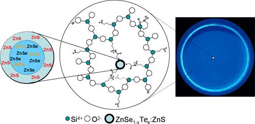 |
| Left: Illustrations of nanoparticles prepared by the addition of Te (inside) and S (outside) elements. Center: Illustrations of nanoparticles dispersed in glass matrix. Right: Blue luminescent images of the prepared glass irradiated with an ultraviolet light. (Source: AIST)
|
|
Semiconductor nanoparticles have been expected to find their applications in various fields as new phosphors, but one obstacle is most of these semiconductor nanoparticles contain cadmium, which is harmful to the human body. On the other hand, ZnSe nanoparticles were known to exhibit emission peak in the ultraviolet region. In this report, researchers have succeeded in tuning the emission peak wavelength of ZnSe nanoparticles in to blue-color region by adding an appropriate amount of Te element to ZnSe nanoparticles and further forming core-shell structure by coating ZnS on the surface of nanoparticles.
|
|
Moreover, the researchers have developed a novel and facile method (layer-by-layer self-assembly (LbL) method) for preparing glass thin-film phosphors utilizing self-organization effect, and succeeded in dispersing the nanoparticles in the films to extremely high concentration (0.01 mol/l). The brightness of the prepared thin films has been dramatically enhanced to up to 30 times of that of conventional phosphor (Y2O2S:Eu) at the same sample thickness. These prepared thin films are expected to be applicable in displays and illuminations as phosphors.
|