Showing Spotlights 353 - 360 of 624 in category All (newest first):
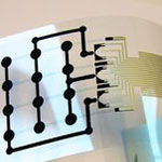 Printed electronics is one of the most important new enabling technologies. It will have a major impact on most business activities from publishing and security printing to healthcare, automotive, military and consumer packaged goods sectors. With recent advances, power and energy storage can be integrated into the printing process, making their potential applications even more ubiquitous. Currently, though, the more complex printed components that require a combination of different class of devices, still experience drawbacks in performance, cost, and large-scale manufacturability. Researchers have now succeeded in fabricating a multi-component sensor array by simple printing techniques - all components (polymer sensor array, organic transistors, electrochromic display) are integrated on the same flexible substrate.
Apr 13th, 2011
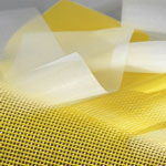 In order to find replacement materials for ITO, scientists have been working with carbon nanotubes, graphene, and other nanoscale materials such as nanowires. While many of these approaches work fine in the lab, upscaleability usually has been an issue. Researchers at Empa, the Swiss Federal Laboratories for Material Science and Technology, have now demonstrated another solution: they presented a transparent and flexible electrode based on a precision fabric with metal and polymer fibers woven into a mesh. The team demonstrated organic solar cells fabricated on their flexible precision fabrics as well as on conventional glass/ITO substrates and found very similar performance characteristics.
Apr 4th, 2011
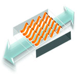
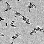 The power conversion efficiency of solar cells made of conjugated polymer/nanorod nanocomposites can be maximized when the nanocomposites are aligned perpendicularly between two electrodes for effective exciton dissociation and transport. To realize this, external fields can be applied to induce the self-assembly/alignment. The challenge is how to assemble them over a large scale - current self-assembly studies of cadmium selenide nanorods in literature are limited to only a micrometer scale. New design approaches are therefore needed to solve this problem. Due to their intrinsic structural anisotropy, nanorods possess many unique properties that make them potentially better nanocrystals than quantum dots for photovoltaics and biomedical applications.
Mar 29th, 2011
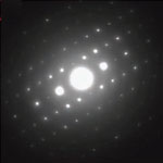
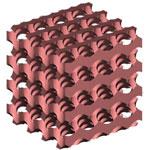 Photonic crystals are used to guide and localize light for all-optical processing of signals/information; to engineer dispersion and slow light; to harvest light (collect and redirect); and thresholdless lasing, that can be engineered by setting spectral ranges where light can be emitted. so far, there have been no demonstrations of full photonic bandgap at visible wavelengths - i.e., that at a certain visible range (between 400 nm to 780 nm) determined by the 3D photonic crystal structure, the light is rejected (reflected) at all angles of incidence. Researchers have now used a 3D nano-sculpturing process to fabricate 3D photonic crystal. The great potential of these 3D photonic crystal lies in the possibility to control light on a sub-wavelength scale.
Mar 23rd, 2011
 Although organic semiconductor materials cannot yet be packed as densely as state-of-the-art silicon chips, they require less power, cost less and do things silicon devices cannot: bend and fold, for example. Once perfected, organic semiconductors will permit the construction of low-cost, spray-on solar cells and even spray-on video displays. Notwithstanding tremendous progress in the area of organic electronics, several major challenges still exist. To address these challenges, researchers have combined organic electronics with nanoelectronics and developed the first 2D crystal of organic semiconductors on the millimeter scale, the thickness of which is only a single molecular layer, but with perfect long-ranged crystalline order.
Mar 15th, 2011
 Currently, the most common methods for sizing nanoparticles extract data from bulk measurements. These techniques are inherently averaging and so are unable to effectively resolve mixtures of different-sized particles. While individual nanoparticles can be sized using electron microscopy, this approach is time-consuming and of little utility in assembling significant population statistics. Researchers have now developed a microfluidic device for the all-electronic analysis of complex suspensions of nanoparticles in fluid. This device is capable of detecting and sizing individual and unlabeled particles as small as a few tens of nanometers in diameter at rates estimated to exceed 100,000 particles per second.
Mar 7th, 2011
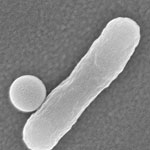 Bacterial propulsion systems are intriguing for nanotechnology researchers because nature has already solved most of the problems that they are still struggling with in designing molecular motors and other self-sustained nanoscale actuating systems. Indeed, it has turned out to be very challenging to even move sub-micron scale structures in well directed paths, especially under biologically friendly conditions. In previous work, researchers have already shown how large numbers of bacteria can propel larger sub-mm scale structures. And in a 2005 paper, researchers demonstrated a method of using the power generated by biological motors to transport microscale loads while leaving these motors in intact cells. Scientists at Johns Hopkins University have now demonstrated a strategy to autonomously move nanostructures in well defined paths by enabling individual bacteria-cargo conjugates. They showed how approximately 500 nm-sized structures deposited on substrates can be attached to individual bacteria and when released, the bacteria stay motile and ferry this cargo.
Mar 1st, 2011
 Previous research has shown that high performance piezoelectric ceramics PZT (lead zirconate titanate) could be printed as nanoribbons onto biocompatible and flexible substrates for applications such as harvesting energy from human motion like walking or breathing. While some motions, such as walking, only require flexibility, others, such as breathing, require that the materials be not just flexible but also stretchable. However, the PZT ribbons cannot stand stretching operation modes due to their brittle nature, which leads to cracking. The research team therefore has been looking to overcome this difficulty by fashioning the piezoelectric ribbons into wavy shapes, and integrating them with stretchable silicone rubber, such that the composite material can withstand large amounts of elastic strain.
Feb 18th, 2011
 Subscribe to our Nanotechnology Spotlight feed