Showing Spotlights 337 - 344 of 624 in category All (newest first):
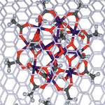
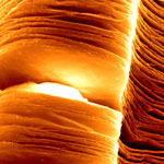 Clean and affordable energy generation and storage is one of the most significant challenges that our world is facing in the 21st century. Materials are going to play a crucial role in generation and storage of renewable energy. While searching for new materials for electrical energy storage, materials scientists have discovered a new family of two-dimensional compounds proposed to have unique properties that may lead to ground-breaking advances in energy storage technology. Researchers transformed three dimensional titanium-aluminum carbide into a two dimensional structure with greatly different properties. This work opens the door for a wide range of metal carbide and/or nitride compositions in form of 2-D sheets.
Aug 29th, 2011
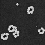 DNA origami is a design technique that is used by nanotechnology researchers to fold DNA strands into something resembling a programmable pegboard on which different nanocomponents can be attached. These DNA assemblies allow the bottom-up fabrication of complex nanostructures with arbitrary shapes and patterns on a 100 nm scale. For instance, DNA origami have been heralded as a potential breakthrough for the creation of nanoscale circuits and devices. DNA can also be metallized with different metals, resulting in conducting nanowires. Researchers have now have developed a method to assemble metallic nanocircuits with arbitrary shapes, by attaching metallic nanoparticles to select locations of the DNA origami and then fusing them to form wires, rings, or any other complex shape. These pre-designed structures are programmed by fully utilizing the self-assembling and recognition properties of DNA.
Aug 11th, 2011
 Super-tough materials with exceptional mechanical properties are in critical need for applications under extreme conditions such as jet engines, power turbines, catalytic heat exchangers, military armors, airplanes, and spacecraft. Researchers involved in improving man-made composite materials are trying to understand how some of the amazing high-performance materials found in nature can be copied or even improved upon. Nature has evolved complex bottom-up methods for fabricating ordered nanostructured materials that often have extraordinary mechanical strength and toughness. The main problem in making nanocomposite materials is how the separate components can be interfaced without losing the good properties of each component. Researchers were now able to show that biomolecules that may seem soft and fragile can actually strengthen a composite material by creating cohesion between two materials that differ much from each other.
Aug 8th, 2011
 Exotic artificial composite materials called metamaterials can be engineered with certain electromagnetic properties that allows them to act as invisibility cloaks. These materials bend all light or other electromagnetic waves around an object hidden inside a metamaterial cloak, to emerge on the other side as if they had passed through an empty volume of space. Researchers have already been experimenting with cloaking devices for various, usually longer wavelengths such as microwave or infrared waves. Recently, even graphene has been added to the family of cloaking materials. Now, for the first time, a team of scientists at UC Berkeley have devised an invisibility cloak material that hides objects from detection using light that is visible to humans.
Aug 3rd, 2011
 Structural color - where the color results from interferences, not pigments - is a natural fit for new display technologies and writing substrates since it can provide vivid colors in environments of high intensity light (e.g. sunlight) without the need for additional illuminating power. Most existing display technologies such as LCDs and LEDs require power to actively project colors and often suffer from performance degradations in these reflective environments. Recognizing this, researchers have developed a number of techniques for dynamically and spatially modulating the colors reflected off of photonic crystal-like substrates. In new work, researchers have demonstrated an electrical-power-free infusion technique that allows them to draw multi-color images on colloidal photonic crystal substrates using transparent imaging oils.
Aug 2nd, 2011
 Single-molecule magnets (SMM) are fascinating nanoscale structures with unique functional properties showing promise for high-density electronic data storage devices, solid state quantum computers, spintronic devices such as spin valves, and other advanced technological applications. Despite a flurry of research in this area - since an individual magnetic molecule represents the ultimate size limit to storing and processing information - the main challenge related to harnessing properties of SMM remained unsolved. A new study by a group of European researchers reports the successful encapsulation of single-molecule magnets in carbon nanotubes, yielding a new type of hybrid nanostructure that combines all the key single-molecule magnet properties of the guest molecules with the functional properties of the host CNT.
Jul 27th, 2011
 To build microprocessors with more than one billion transistors, manufacturers still use the same technique - photolithography, the high-tech, nanoscale version of printing technology - that they have been using for the past 50 years. State-of-the-art photolithography processes use 193 nm light to produce diffraction-limited features as small as 32 nm. Going beyond 32 nm, the cost and complexity rises significantly, posing massive technological and economic challenges for chip manufacturers. This provides plenty of incentives for researchers to explore alternative manufacturing technologies for chipmakers. One novel approach is based on the use of DNA nanostructures to pattern a silicon wafer.
Jul 26th, 2011
 For more than 5000 years, noble metals have been known to be impervious to magnetic fields. Significant scientific breakthroughs in the recent past have led to making either 13 atoms clusters of platinum or organic molecule capped noble metal nanoparticles magnetic. By carefully controlling the size, shape, and composition of noble metals - especially in confined nanoscale systems - their properties can be modified, potentially leading to significantly advanced nanomaterial-based applications such as catalysis, self-assembly, novel metamaterials, improved MRI research, and spintronics. Now, researchers have developed simple method to make nano- and macro-particles of noble metals magnetic.
Jul 12th, 2011
 Subscribe to our Nanotechnology Spotlight feed