Showing Spotlights 329 - 336 of 624 in category All (newest first):
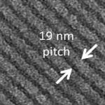
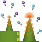
 Directed self-assembly of block copolymers is a candidate lithography for use in future nanoelectronics and patterned media copolymer with resolutions down to the sub-10nm domain. Variations of this effective nanofabrication technique have been used to write periodic arrays of nanoscale features into substrates at exceptionally high densities with resolutions that are difficult or impossible to achieve with top-down techniques alone. However, in many cases these approaches are either too costly or too complex due to the required number of processing steps, for instance expensive, time-consuming substrate pre-patterning. Researchers at the Molecular Foundry have now shown that block copolymers can be aligned on an unpatterned substrate using a removable and reusable mold applied from above.
Dec 5th, 2011
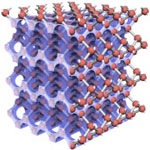 There is a lot of buzz in the computer industry about so-called three-dimensional (3D) chips, promising higher performance with lower energy consumption, and paving the way for exascale computers (which would represent a thousandfold increase in performance over the current petascale architecture). However, these chips are not intrinsically built, true 3D chips; rather, they are stacked layers of up to 100 separate chips. In a major breakthrough in the field of photonic crystals, researchers in The Netherlands have developed a novel process that allows for rapid fabrication of large 3D photonic crystals in mono-crystalline silicon using CMOS compatible processes.
Nov 17th, 2011
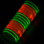 Conventional microfluidic devices are fabricated in inherently planar, block-like devices. In contrast, an important feature of naturally self-assembled systems such as leaves and tissues is that they are curved and have embedded fluidic channels that enable the transport of nutrients to, or removal of waste from, specific three-dimensional regions. Since most microfluidic devices are created using layer-by-layer lithographic patterning and molding methods, it is challenging to create microfluidic networks in curved or folded geometries. However, such networks are important to pattern chemicals in 3D and also to create realistic models of tissues. Researchers have now demonstrated, for the first time, a strategy to self-assemble curved and folded microfluidic polymeric devices with materials used in conventional planar, microfluidics namely SU8 and PDMS.
Nov 14th, 2011
 Cost of ownership has become a critical challenge facing future research in nanofabrication. As potential applications have broadened beyond the high-volume manufacture of integrated circuits, demand has increased for a robust tool capable of lithography at high pattern density and fidelity but also at low cost and thus suitable for scientific research, rapid prototyping, and low-volume manufacturing. Unfortunately, current manufacturing technologies employed in the chip industry are anything but 'low cost'. Researchers have now demonstrated a new source for lithography that has both higher per-particle exposure efficiency and a higher brightness than the sources conventionally used for lithography at the 10 nm scale.
Oct 11th, 2011
 A single drop of water can be fatal to electrical circuits. To prevent water damage, current electronic devices are well sealed and packaged with polymer passivation. Researchers in Korea have now gone one step further and made water resistance a feature of the device itself by incorporating nonwetting, superhydrophobic components into the electronic device. They demonstrated this novel idea with a source/drain structure in a thin-film transistor. This work combines superhydorphobicity with electronic devices, especially resistive switching memory devices. Although much research has been done on either topic, few works report the combination of combining superhydrophobicity and electronic devices. This is a novel approach to combine two different concepts to get a synergic effects.
Oct 5th, 2011
 In recent years various bottom-up processes (such as growth techniques) and top-down processes (such as electron beam, lithography, nanoimprint) have been used to produce one dimensional nanostructure on semiconductor substrate. All these approaches involve nanoscale prepatterning or extreme fabrication conditions; hence, they are often limited by associated high cost and low yield. In a novel nanomanufacturing process known as Simultaneous Plasma-Enhanced Reactive Ion Synthesis and Etching (SPERISE), researchers have integrated both nanoscale bottom-up synthetic and top-down etching approach. This eliminates the expensive prepatterning steps and hence give rise to ultrahigh throughput, better reliability, high yield and above all, low cost.
Oct 3rd, 2011
 Along with graphene, atomically thin sheets and ribbons of boron nitride (often called "white graphene") have increasingly attracted fundamental research interest. While researchers make good progress on developing techniques for mass-producing graphene, it is still a challenge to reliably chemically delaminate and/or exfoliate boron nitride and to realize mass production of atomically thin sheets made of this material. Researchers in Japan have now reported a new approach for synthesizing boron nitride monolayers which pretty much works like blowing a balloon; although these balloons are sized in a range of tens of micrometers. The new technique solves the problem of low-throughput fabrication of 2D crystals.
Sep 19th, 2011
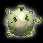 Bio-conjugated nanoparticles are important analytical tools with emerging biological and medical applications. Especially gold nanoparticles are of increasing interest for nanobiotechnology research and applications because of their high acceptance level in living systems and the fact that they are fairly easily conjugated with functional molecules. Ultrashort pulsed laser ablation represents a powerful tool for the generation of pure gold nanoparticles avoiding chemical precursors, reducing agents, and stabilizing ligands. The bare surface of the charged nanoparticles makes them highly available for functionalization and as a result especially interesting for biomedical applications. Starting today, such conjugates are available commercially for the first time.
Sep 15th, 2011
 Subscribe to our Nanotechnology Spotlight feed