Showing Spotlights 25 - 32 of 41 in category All (newest first):
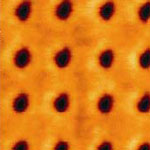
 Even though traditional, digital computers have consistently increased in speed and complexity, they are limited by their reliance on sequential processing of instructions; i.e. no matter haw fast they are, they still process only one bit at a time. By contrast, individual neurons in our brain are very slow: they fire at only about 1000 times per second; however, since they are operating in a massively parallel way, with millions of neurons working collectively, they are able to complete certain tasks more efficiently than even the fastest super-computer. Another important distinction of our brain is that, during computing, information processing circuits evolve continuously to solve complex problems. An international research team from Japan and Michigan Technological University has now created a similar process of circuit evolution in an organic molecular layer, which also solves complex problems. This brain-like 'evolutionary' circuit has been realized for the first time in the world.
Apr 26th, 2010
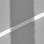
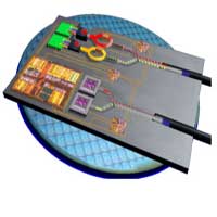
 In developing next generation data storage devices, researchers are employing a variety of nanotechnology fabrication and patterning techniques such as electron-beam lithography, photolithography, microcontact printing, nanoimprinting and scanning probe microscope-based lithography. A decade ago, IBM for instance introduced the Millipede Project, a thermomechanical AFM-based nanopatterning technique that was aimed at data storage systems. While this system required an AFM tip heated to 350 degrees centigrade, researchers in Korea have now demonstrated that the writing, reading, and erasure of nanoscopic indentations on a polymeric film can be achieved by using an AFM tip at room temperature - no heating required.
Sep 18th, 2009
 Experiments with graphene have revealed some fascinating phenomena that excite researchers who are working towards molecular electronics. It was found that graphene remains capable of conducting electricity even at the limit of nominally zero carrier concentration because the electrons don't seem to slow down or localize. This means that graphene never stops conducting. Taking advantage of the conducting properties of graphene, researchers now have described how graphene memory could potentially be used as a new type of memory that could significantly exceed the performance of current state-of-the-art flash memory technology. Their results show the possibility to build next-generation memory devices with vast amounts of memory using nanocables with a silicon dioxide core and a shell of stacked sheets of graphene.
Nov 25th, 2008
 The method that has been traditionally used in binary information storage is by making a distinction between storage (designated as 1) and non-storage (designated as 0). In reality, each imprint (or non-imprint) can store either 1 or 0. Thus the sequence and the numbers of 1 and 0 define everything with respect to the amount of information that can be stored and retrieved at the hardware level, no matter how sophisticated the overlaying software routines are. Ever since computers were developed, information storage has adhered to the eight-bit system. No matter how sophisticated information storage technologies have become - exploiting magnetoresistance, developing optical storage media such as CDs, DVDs and blue-ray discs, or the development of holographic storage media - a bit is always represented by manipulating a single feature, i.e., a transition or non-transition. Now, in contrast, consider the following: There are four colors, each of which could at least represent two or more bits; whereas in conventional methods only a single bit is available. In terms of color, this is somewhat similar to a black and white system that can support at most two kinds of transitions - 0 to 1 and 1 to 0. On the other hand, in four-color coded systems there can be 16 such unique transitions.
Oct 23rd, 2008
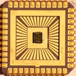 For nanoelectronics applications like single-electron devices to become practical, everyday items, they need to move from the highly individual and customized fabrication process typically found in laboratories to an automated, high-throughput and industrial-scale production environment. The reason this hasn't happened yet is that the various nanoscale pattern definition techniques used today - such as e-beam lithography, mechanically controllable break junctions, electromigration, electrodeposition, nanoscale oxidation, and scanning tunneling microscopy - generally are not suitable for large-scale parallel processing. The fabrication of single-electron devices requires nanoscale geometrical arrangement of device components, that is, source and drain electrodes and Coulomb islands. Developing methods to fabricate nanoscale devices in large numbers at a time has been one of the major efforts of the nanotechnology community. A new study now demonstrates that this can be done with complete parallel processing using CMOS-compatible processes and materials. Furthermore, these single-electron devices can operate at room temperature, an essential requirement for practical implementations.
Sep 18th, 2008
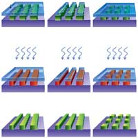 In the past, random defects caused by particle contamination were the dominant reason for yield loss in the semiconductor industry - defects occur in the patterning process (so-called process defects) when contaminants become lodged in or on the wafer surface. Trying to prevent such fabrication defects, chip manufacturers have spent much effort and money to improve the fabrication process, for instance by installing ultra-clean fabrication facilities. With the semiconductor industry's move to advanced nanometer nodes, and feature sizes approaches the limitation of the fabrication method used, particles are no longer the only problem for chip manufacturers. In a nanoscale feature-size fabrication environment, systematic variations, such as metal width and thickness variations or mask misalignment, are also major contributors to yield loss. Rather than perfecting a nanostructure by improving its original fabrication method, researchers at Princeton University have demonstrated a new method, known as self-perfection by liquefaction (SPEL), which removes nanostructure fabrication defects and improves nanostructures after fabrication.
May 4th, 2008
 In its everlasting quest to deliver more data faster and on smaller components, the silicon industry is moving full steam ahead towards its final frontiers of size, device integration and complexity. We have covered this issue numerous times in previous Spotlights. As the physical limitations of metallic interconnects begin to threaten the semiconductor industry's future, one group of researchers and companies is betting heavily on advances in photonics that will lead to combining existing silicon infrastructure with optical communications technology, and a merger of electronics and photonics into one integrated dual-functional device. Today, silicon underpins nearly all microelectronics but the end of the road for this technology has clearly come into view. Photonics is the technology of signal processing, transmission and detection where the signal is carried by photons (light) and it is already heavily used in photonic devices such as lasers, waveguides or optical fibers. Optical technology has always suffered from its reputation for being an expensive solution, due to its use of exotic materials and expensive manufacturing processes. This prompted research into using more common materials, such as silicon, for the fabrication of photonic components, hence the name silicon photonics. Although fiber-optic communication is a well-established technology for information transmission, the challenge for silicon photonics is to manufacture low-cost information processing components. Rather than building an entirely new industrial infrastructure from scratch, the goal here is to to develop silicon photonic devices manufactured using standard CMOS techniques. A recent review paper takes a look at the state of silicon photonics and identifies the challenges that remain on the path to commercialization.
Mar 14th, 2008
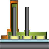 A memory chip is an integrated circuit made of millions of transistors and capacitors. In the most common form of computer memory, dynamic random access memory (DRAM), a transistor and a capacitor are paired to create one memory cell, which represents a single bit of data. The capacitor holds the bit of information, either a 0 or a 1. The transistor acts as a switch that lets the control circuitry on the memory chip read the capacitor or change its state. Because each bit stored in a chip is controlled by one transistor, memory capacities tend to expand at the same pace as the number of transistors per chip - which still follows Moore's Law and therefore currently doubles every 18 months. The problem is that the capacitor - consisting of two charged layers separated by an insulator - can shrink only so far. The thinner insulators get the more they allow charges to tunnel through. Tunneling increases the leakage current, and therefore the standby power consumption. Eventually the insulator will break down. Researchers have been trying to develop electromechanically driven switches that can be made small enough to be an alternative to transistor-switched silicon-based memory. Electromechanical devices are suitable for memory applications because of their excellent ON-OFF ratios and fast switching characteristics. With a mechanical switch there is physical separation of the switch from the capacitor. This makes the data leakage problem much less severe. Unfortunately they involve larger cells and more complex fabrication processes than silicon-based arrangements and therefore have not been so far an alternative to scaling down beyond semiconductor transistors. Researchers now have reported a novel nanoelectromechanical (NEM) switched capacitor structure based on vertically aligned multiwalled carbon nanotubes (CNTs) in which the mechanical movement of a nanotube relative to a carbon nanotube based capacitor defines ON and OFF states.
Jan 10th, 2008
 Subscribe to our Nanotechnology Spotlight feed