Showing Spotlights 1681 - 1688 of 2780 in category All (newest first):
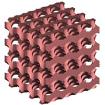 Photonic crystals are used to guide and localize light for all-optical processing of signals/information; to engineer dispersion and slow light; to harvest light (collect and redirect); and thresholdless lasing, that can be engineered by setting spectral ranges where light can be emitted. so far, there have been no demonstrations of full photonic bandgap at visible wavelengths - i.e., that at a certain visible range (between 400 nm to 780 nm) determined by the 3D photonic crystal structure, the light is rejected (reflected) at all angles of incidence. Researchers have now used a 3D nano-sculpturing process to fabricate 3D photonic crystal. The great potential of these 3D photonic crystal lies in the possibility to control light on a sub-wavelength scale.
Mar 23rd, 2011
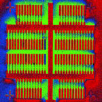 The commercial realization of carbon nanotube-based electronic devices and their integration into the existing silicon-based processor technologies is still hampered by the inability to scale up the - currently lab-based - fabrication processes to manufacture a large number of devices on a single chip. The fundamental issue of carbon nanotube device fabrication still remains the biggest challenge for effective commercialization of nanotube electronics. In a further step towards large-scale integration of single-walled carbon nanotubes (SWCNTs) into complex functional electronic circuits, researchers have now combined a previously developed dielectrophoretic deposition approach with SWCNT sorting using density gradient ultracentrifugation, ensuring high purity of SWCNTs in suspension and consequently in the assembled devices.
Mar 22nd, 2011
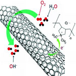 The efficiency of catalyzing the oxygen reduction reaction (ORR) - the process that breaks the bonds of oxygen molecules - to a large degree determines the electrochemical performance of fuel cells. Platinum and platinum-based composites have long been considered as the most efficient ORR catalysts. In their search for practically viable non-precious metal ORR catalysts, researchers have also been investigating vertically-aligned nitrogen-containing carbon nanotubes. Having a strong electron-withdrawing ability, poly(diallyldimethylammonium chloride) (PDDA) was used to create net positive charge for carbon atoms in the nanotube carbon plane via intermolecular charge transfer. The resultant PDDA functionalized/adsorbed carbon nanotubes were demonstrated to act as metal-free catalysts for oxygen reduction reaction in fuel cells with similar performance as platinum catalysts.
Mar 21st, 2011
 In a standard dye sensitized solar cell, an organic molecule adsorbed on the surface of a porous electrode absorbs light and then initiates the charge separation process eventually leading to generation of photocurrent. While the dye appears to have "sensitized" the large bandgap material, it never actually does, because only the dye molecules absorb the light and generate the carriers, the large bandgap material primarily serves the function of a conducting channel to take the electrons out. While wide bandgap materials alone can not absorb the sun light efficiently, it has been predicted that if two large bandgap materials with type-II band alignment form coaxial nanowires, the effective indirect bandgap could be substantially smaller than either of the individual materials. After a few years effort, one research team has now demonstrated a real functional device that exhibits the key feature of the idea: the use of two large bandgap materials to make a solar cell behaving like a small bandgap material.
Mar 18th, 2011
 At the core of research efforts to determine the impact of synthetic nanoparticles on the environment and living systems is a fundamental understanding of the interactions between man-made nanoparticles and natural living systems that have evolved over millions of years. To describe nanoparticles at large, it may be beneficial to acknowledge that 1) biological systems are part of the food chain and therefore an essential component of the ecosystems and 2) collaborations are essential for such interdisciplinary research. Researchers have now presented a biophysical perspective that describes the fate of nanoparticles in both the aqueous phase and in living systems.
Mar 16th, 2011
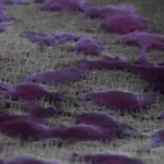
 Although organic semiconductor materials cannot yet be packed as densely as state-of-the-art silicon chips, they require less power, cost less and do things silicon devices cannot: bend and fold, for example. Once perfected, organic semiconductors will permit the construction of low-cost, spray-on solar cells and even spray-on video displays. Notwithstanding tremendous progress in the area of organic electronics, several major challenges still exist. To address these challenges, researchers have combined organic electronics with nanoelectronics and developed the first 2D crystal of organic semiconductors on the millimeter scale, the thickness of which is only a single molecular layer, but with perfect long-ranged crystalline order.
Mar 15th, 2011
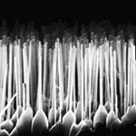
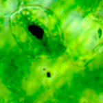
 In order to get a true picture of the processes and events that take place inside unmodified, living cells, probing techniques need to be non-destructive, noninvasive and in real-time. Due to their small dimensions, high-aspect ratio nanomaterials such as nanofibers, nanowires and carbon nanotubes are ideal for cellular applications since they can cross the cell membrane without causing significant damage. In particular, semiconductor nanowires attract a lot of interest because of their uniformity, reproducibility and possibility of fine-tuning their intrinsic properties - physical dimensions, crystal structure, electrical and optical properties, etc. Researchers have now shown, for the first time, the spontaneous and close interface of arrays of vertically aligned indium arsenide nanowires with two relevant cell lines, human embryonic kidney cells and rat embryonic dorsal root ganglion neurons.
Mar 14th, 2011
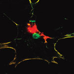 Owing to their large surface area, strong infrared photoluminescence and magnetic properties, nanodiamonds are promising for various biomedical applications, including as drug/gene carriers and alternatives to the current bio-imaging platforms. However, the biomedical applications will hardly be realized unless the potential hazards of nanodiamonds to humans and other biological systems are ascertained. The biocompatibility of nanodiamonds at the cellular level has been confirmed by many independent studies. Following these earlier cytotoxicity studies, many groups have used nanodiamonds and their functionalized derivatives for drug/gene deliveries. In spite of the earlier reports that nanodiamonds are biocompatible at the cellular level, researchers have now demonstrated in a new study that nanodiamonds can activate DNA repair proteins in embryonic stem cells, suggesting possible DNA damages.
Mar 10th, 2011
 Subscribe to our Nanotechnology Spotlight feed