Showing Spotlights 1641 - 1648 of 2784 in category All (newest first):
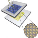 Paper has emerged as a focus area for researchers developing innovative techniques for printed basic electronics components. Another area where paper could lead to low-cost innovative devices and applications is lab-on-a-chip technology. Currently, these microfluidic devices are fairly expensive due to their lithography-based fabrication process with channels patterned in glass or plastic and tiny pumps and valves directing the flow of fluids. Inexpensive paper-based sensing kits already play an important role in ready-to-use diagnostics. Researchers have even managed to create inexpensive microfluidic platforms on hydrophobic paper with laser treatments. In a further advance, scientists have now fabricated a paper-based metamaterial device which can be potentially utilized for quantitative analysis in biochemical sensing applications.
Jun 20th, 2011
 Radiation damage to materials is a major issue for builders of nuclear power plants as well as spacecraft engineers. The former have to worry about material failure due to the destructive radiation created within the reactor; the later are concerned about the exposure to space radiation of both materials and humans during long-term space missions. There is a consensus that interface engineering is the way to go to to improve resistance to extreme conditions in general and to reach radiation tolerance in particular - interfaces are places where defects created by energetic collision in solids can annihilate each other and thus render the material immune to irradiation. All kind of interfaces are being explored, in particular those formed by the contact between two different solid state phases.
Jun 15th, 2011
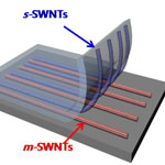 Current production methods for carbon nanotubes (CNTs) result in units with different diameter, length, chirality and electronic properties, all packed together in bundles, and often blended with some amount of amorphous carbon. Often, these mixtures are of little practical use since many advanced applications, especially for nanoelectronics, are sensitively dependent on the structures. Separation of nanotubes according to desired properties is still proving to be a challenging task, especially single-walled carbon nanotube (SWCNT) sorting. The composition of SWCNTs of different types is very similar, but the chemical properties are not. Conventional separation techniques are efficient in separation of carbon nanotubes, but there are many drawbacks. Researchers in Asia have now developed a simple way to realize the separation of single-walled carbon nanotubes via the interaction difference between chemicals and carbon nanotubes.
Jun 14th, 2011
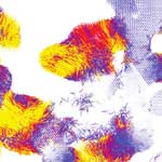
 Graphene has two distinct types of edges produced when it is cut - armchair type or zigzag type - which correspond to the two crystal axis of graphene. These edge types have distinct electronic, magnetic, and chemical properties, and being able to pattern graphene along particular crystallographic directions to leave edges consisting of a single chirality is crucial for the fabrication of graphene nanoribbon and nanoelectronics devices. A widely discussed method for the patterning of graphene is the channelling of graphite by metal nanoparticles in oxidizing or reducing environments. Researchers now report the live nanoscale observation of this channelling process by silver nanoparticles.
Jun 13th, 2011
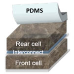 Apart from making graphene, graphene oxide itself itself is a fascinating material that has many intriguing properties. Researchers have now developed a graphene-based conductive glue that can function as a metal-free solder for creating mechanical and electrical connections in organic optoelectronic devices. As a proof-of-concept, they fabricated polymer tandem solar cells - multi-junction photovoltaic devices, in which two sub-cells are stacked to achieve higher overall solar absorption - by a direct 'gluing' process. The water-based sticky interconnect and the associated adhesive lamination process could transform the serial layer-by-layer fabrication of tandem devices into a parallel mode, in which the subcells can be independently fabricated and adjusted to balance their photocurrents for achieving high efficiency.
Jun 10th, 2011
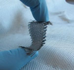 The future of your shirts, socks and gloves will be electronic. In years to come, wearable electronics will look nothing like even your smallest iPod or mobile phone today. Not only will such devices be embedded on textile substrates, but an electronics device or system could become the fabric itself. Here is some recent work that demonstrates the kind of issues scientists are working on today and that will help improve the performance of electronic textile structures. Using atomic layer deposition (ALD), researchers have grown coatings of inorganic materials on the surface of textiles like woven cotton and nonwoven polypropylene. By fabricating an all-fiber capacitor, they show that their coated materials are sufficiently conductive to perform in simple device architectures.
Jun 9th, 2011
 Unlike silicon, graphene lacks an electronic band gap - the gap being an energy range that cannot be occupied by electrons - and therefore has no switching capability; which is essential for electronics applications. Opening an energy gap in graphene's electron energy spectrum is therefore a critical prerequisite for instance for creating graphene transistors. That's where strain engineering of graphene comes in. Researchers have discovered that local strain in a graphene sheet can alter its conducting properties. By varying the amount of local strain, transport gaps can be tailored. In new work, researchers present a new and novel mechanism for gap opening in strained graphene via electrostatic gates and show that it can be important also in realistic situations.
Jun 8th, 2011
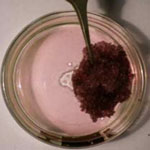 Water treatment is important for human consumption and environmental protection. Non-trivial purification of water involves removal of toxic ions, organic impurities, microbes and their by-products as well as scooping oil spills. The removal of organic contaminants from water is a major industrial concern. The challenging goal here is to detect, decompose and remove contaminants present usually in low concentrations. Towards this end, different types of sorbent materials have been developed to date, the most common being activated carbon. Though the use of activated carbon is still considered to be one of the best method, the disposal of adsorbed contaminants along with the adsorbent is a major concern. Researchers in India have recently come up with an innovative method for organic pollutant removal from waste water.
Jun 7th, 2011
 Subscribe to our Nanotechnology Spotlight feed